Stacking of Bi2Te3 and FeSi2 for Thermoelectric Applications

Article Preview

Abstract:

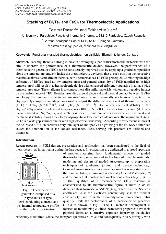
Recently, there is a strong interest in developing superior thermoelectric materials with the aim to improve the performance of a thermoelectric device. However, the performance of a thermoelectric generator (TEG) can be considerably improved also by applying a graded composition along the temperature gradient inside the thermoelectric device so that at each position the respective material achieves its maximum thermoelectric performance (TE FGM principle). Combining the high efficiency of Bi2Te3 (used at low temperatures) and general durability of FeSi2 (applied up to high temperatures) will result in a thermoelectric device with enhanced efficiency operating in air at a wide temperature range. The challenge is to contact these dissimilar materials without any negative impact on the performance of TEG. Besides providing a good electrical and thermal contact between Bi2Te3 and FeSi2 the junctions have to remain mechanically and chemically stable over long term. A Bi2Te3-SiO2 composite interlayer was used to adjust the different coefficient of thermal expansion (CTE) of FeSi2 (≈ 7·10-6 K-1) and Bi2Te3 (≈ 19·10-6 K-1). Due to low chemical stability of the Bi2Te3/FeSi2 contact at elevated temperatures (1000 h @ 300°C) a contacting material (diffusion barrier) based on Ni, Zn, Ti, and ZnTe was tested. Some contacts show excellent chemical and mechanical stability, though the electrical properties of the contacts do not meet the requirements (e.g. ZnTe is a wide gap semiconductor with high electrical resistivity). According to very recent studies at the Zn-based diffusion barriers a very thin layer of undoped ZnTe growing at the Bi2Te3/Zn interface causes the deterioration of the contact resistance. Ideas solving this problem are outlined and discussed.

You might also be interested in these eBooks

Info:

Periodical:

Materials Science Forum (Volumes 492-493)

Pages:

273-280

Citation:

Online since:

August 2005

Export:

Price:

Permissions CCC:

Permissions PLS:

Сopyright:

© 2005 Trans Tech Publications Ltd. All Rights Reserved

Share:

Citation:

[1] A. Iwama, H. Kohri and I. Shiota: Functionally Graded Materials 2002, Proc. of the 7th Int. Symposium on Functionally Graded Materials, Beijing, China, Oct. 15-18, 2002 (Trans Tech Publications., Switzerland, 2003).

Google Scholar

[2] K. Trumble, K. Bowman, I. Reimanis, S. Sampath: Functionally Graded Materials 2000, Proc. of the 6th Int. Symp. on Functionally Graded Materials, Estes Park, CO, USA, Sept. 10-14, 2000 (Ceramic Transactions 114, The American Ceramic Society, 2001).

Google Scholar

[3] I. Shiota, I. A. Nishida: Proc. 16th Int. Conf. on Thermoelectrics, Dresden, Germany, Aug. 26-29, 1997, IEEE, Piscataway, NJ, 1997, p.364.

Google Scholar

[4] R. R. Heikes, R. W. Ure, Jr.: Chapter 1, Thermoelectricity: Science and Engineering (Interscience Publishers, R. R. Heikes, R. W. Ure Jr. Eds., New York - London, 1961).

DOI: 10.1021/ed039p274.1

Google Scholar

[5] H. J. Goldsmid: Chapter 3, CRC Handbook of Thermoelectricity (CRC Press Boca Raton, D. M. Rowe Ed., New York, London, Tokyo, 1995).

Google Scholar

[6] A. F. Ioffe: Pat. USSR No. 126158, Byulleten' izobretenii (Invention Review) 4 (1960) p.22 (in Russian).

Google Scholar

[7] T. Hirano, L. W. Whitlow, M. Miyajima: Functionally Gradient Materials (Ceramic Transactions 34, The American Ceramic Soc. J. B. Holt, M. Koizumi, T. Hirai, Z. A. Munir Eds., 1993), p.23.

Google Scholar

[8] K. Eguchi: FGM News 28 (1995) p.1.

Google Scholar

[9] Y. Miyamoto, M. Niino, M. Koizumi, Proc. 4th Int. Symp. on FGM, Tsukuba, Japan, Oct. 21-24, 1996 (Elsevier, Amsterdam, 1997), p.1.

Google Scholar

[10] Y. S. Kang, M. Niino, I. A. Nishida, and J. Yoshino: Proc. 17th Int. Conf. on Thermoelectrics, Nagoya, Japan, May 24-28, 1998, IEEE, Piscataway, NJ 1999, p.429.

Google Scholar

[11] C. Drasar, A. Mrotzek, Ch. Stiewe, E. Müller and W.A. Kaysser: Functionally Graded Materials 2002, Proc. of the 7th Int. Symp. on Functionally Graded Materials, Beijing, China, Trans Tech Publications, 2003, p.391.

Google Scholar

[12] W. Kuhn, H. P. Wagner, H. Stanzl, K. Wolf, K. Worle, S. Lankes, J. Betz, M. Worz, D. Lichtenberger, H. Leiderer, W. Gebhardt and R. Triboulet, Semicond. Sci. Technol. Vol. 6 (1991), A105-A108.

DOI: 10.1088/0268-1242/6/9a/019

Google Scholar

[13] R. M. Park, M. B. Troffer, C. M. Rouleau, J. M. DePuydt and M. A. Haase, Appl. Phys. Lett. Vol. 57 (1990), p.2127.

Google Scholar