Laser Induced Etching for Generation of Si Nanocrystals and Spectroscopic Investigation of Morphology

Article Preview

Abstract:

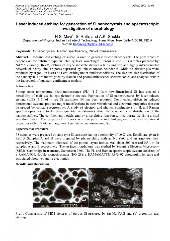
Laser-induced etching of silicon is used to generate silicon nanocrystals. The pore structure depends on the substrate type and etching laser wavelength. Porous silicon (PS) samples prepared by Nd:YAG laser (1.16 eV) etching of n-type substrate showed a fairly uniform and highly interconnected network of nearly circular pores separated by thin columnar boundaries, while no circular pits were produced by argon- ion laser (2.41 eV) etching under similar conditions. The size and size distribution of the nanocrystals are investigated by Raman and photoluminescence spectroscopies and analyzed within the framework of quantum confinement models.

You might also be interested in these eBooks

Info:

Pages:

43-46

Citation:

Online since:

January 2005

Export:

Price:

Permissions CCC:

Permissions PLS:

Сopyright:

© 2005 Trans Tech Publications Ltd. All Rights Reserved

Share:

Citation:

[1] L.T. Canham: Appl. Phys. Lett. Vol. 75 (1990), p.1046.

Google Scholar

[2] N. Noguchi, I. Suemune: Appl. Phys. Lett. Vol. 62 (1993), p.1429.

Google Scholar

[3] B.G. Rasheed, H.S. Mavi, A.K. Shukla, S.C. Abbi, K.P. Jain: Mat. Sci. & Eng. B. Vol. 79 (2001) p.71.

Google Scholar

[4] K.W. Kolasinski, C.J. Barnard, S. Ganguly, L. Koker, A. Wellner, M. Aindow, R.E. Palmer, C.N. Field, P.A. Hamley, M. Poliakoff: J. Appl. Phys. Vol. 88 (2000), p.2472.

DOI: 10.1063/1.1287770

Google Scholar

[5] H.S. Mavi, B.G. Rasheed, A.K. Shukla. S.C. Abbi, K.P. Jain: J. Phys. D: Appl. Phys. Vol. 34, (2001), p.292.

Google Scholar

[6] H.S. Mavi, B.G. Rasheed, R.K. Soni, S.C. Abbi and K.P. Jain: Thin Solid Films Vol. 397 (2001), p.125.

DOI: 10.1016/s0040-6090(01)01410-9

Google Scholar

[7] T. Suemoto, K. Tanaka, A. Nakajima and T. Itukura: Phys. Rev. Lett. Vol. 70 (1993), p.3659.

Google Scholar

[8] H. Richter, Z.P. Wang, and L. Ley: Solid State Commun. Vol. 39 (1981), p.625.

Google Scholar