Optimum Digital Filter for High-Performance All-Digital Phase-Locked Loop

Article Preview

Abstract:

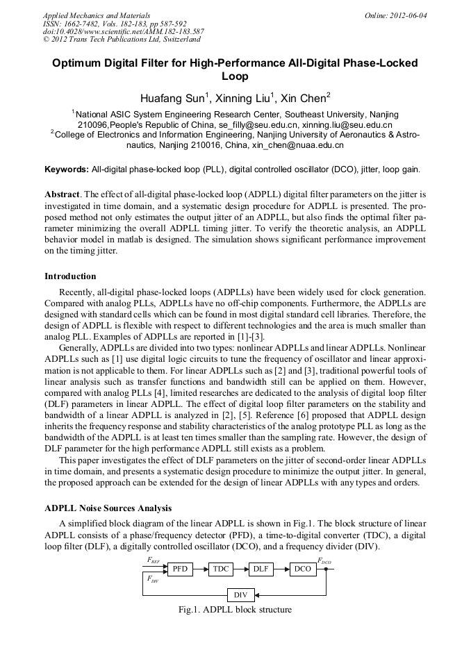
The effect of all-digital phase-locked loop (ADPLL) digital filter parameters on the jitter is investigated in time domain, and a systematic design procedure for ADPLL is presented. The pro-posed method not only estimates the output jitter of an ADPLL, but also finds the optimal filter pa-rameter minimizing the overall ADPLL timing jitter. To verify the theoretic analysis, an ADPLL behavior model in matlab is designed. The simulation shows significant performance improvement on the timing jitter.

You might also be interested in these eBooks

Info:

Periodical:

Pages:

587-592

Citation:

Online since:

June 2012

Export:

Price:

Permissions CCC:

Permissions PLS:

Сopyright:

© 2012 Trans Tech Publications Ltd. All Rights Reserved

Share:

Citation:

[1] Ching-Che Chung, and Chen-Yi Lee, An All-Digital Phase-Locked Loop for High-Speed Clock Generation, IEEE Journal of Solid-State Circuits, vol. 38, no. 2, p.347, (2003).

DOI: 10.1109/jssc.2002.807398

Google Scholar

[2] T. Olsson and P. Nilsson, A Digitally Controlled PLL for SoC Applications, IEEE Journal of Solid-State Circuits, vol. 39, no. 5, p.751, (2004).

DOI: 10.1109/jssc.2004.826333

Google Scholar

[3] R. B. Staszewski and P. T. Balsara, Phase-domain all-digital phase-locked loop, IEEE Trans. Circuits Syst. II, Exp. Briefs, vol. 52, no. 3, p.159, (2005).

DOI: 10.1109/tcsii.2004.842067

Google Scholar

[4] Joonsuk Lee, Beomsup Kim, A Low-Noise Fast-Lock Phase-Locked Loop with Adaptive Bandwidth Control, IEEE Journal of Solid-State Circuits, vol. 35, no. 8, p.1137, (2000).

DOI: 10.1109/4.859502

Google Scholar

[5] A. M. Fahim, A compact, low-power low-jitter digital PLL, in Proc. Eur. Solid-State Circuits Conf., 2003, p.101.

DOI: 10.1109/esscirc.2003.1257082

Google Scholar

[6] Volodymyr Kratyuk, and Pavan Kumar Hanumolu A Design Procedure for All-Digital Phase-Locked Loops Based on a Charge-Pump Phase-Locked Loop Analogy, IEEE Trans. Circuits Syst. II, vol. 54, no. 3, p.247, (2007).

DOI: 10.1109/tcsii.2006.889443

Google Scholar

[7] Asad A. Abidi, Phase Noise and Jitter in CMOS Ring Oscillators, IEEE Journal of Solid-State Circuits, vol. 41, p.1803, (2006).

DOI: 10.1109/jssc.2006.876206

Google Scholar

[8] Floyd M. Gardner, Phaselokc Techniques, New York: John Wiley & Sons, 2005, p.295.

Google Scholar