Efficient Utilization of FPGA Using LUT-6 Architecture

Article Preview

Abstract:

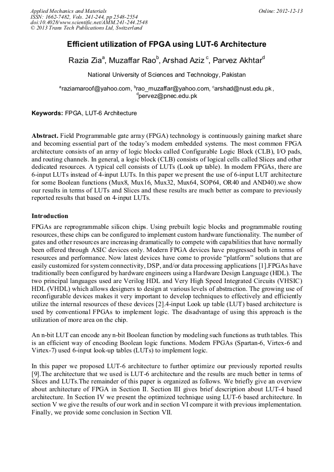
Field Programmable gate array (FPGA) technology is continuously gaining market share and becoming essential part of the today’s modern embedded systems. The most common FPGA architecture consists of an array of logic blocks called Configurable Logic Block (CLB), I/O pads, and routing channels. In general, a logic block (CLB) consists of logical cells called Slices and other dedicated resources. A typical cell consists of LUTs (Look up table). In modern FPGAs, there are 6-input LUTs instead of 4-input LUTs. In this paper we present the use of 6-input LUT architecture for some Boolean functions (Mux8, Mux16, Mux32, Mux64, SOP64, OR40 and AND40).we show our results in terms of LUTs and Slices and these results are much better as compare to previously reported results that based on 4-input LUTs.

You might also be interested in these eBooks

Info:

Periodical:

Pages:

2548-2554

Citation:

Online since:

December 2012

Export:

Price:

Permissions CCC:

Permissions PLS:

Сopyright:

© 2013 Trans Tech Publications Ltd. All Rights Reserved

Share:

Citation:

[1] National Instruments, Introduction to FPGA technology: Top Five Benefits, April 2012. P. 1-2. http://www.ni.com/white-paper/6984/en

Google Scholar

[2] Advantages of FPGA design methodologies, EE Times: july 2004. http://www.design-reuse.com/articles/8404/advantages-of-fpga-design-methodologies.html

Google Scholar

[3] BDTI Focus Report: FPGA for DSP. 2nd ed. BDTI Benchmarking; 2006.

Google Scholar

[4] Latif Kashif, Aziz Arshad, Mahboob. Efficient resource utilization of FPGA. In:FIT'09 proceedings of sixth international conference on Frontiers of information Technology, ISBN:978-1-60558-642-7. New York, USA: ACM;2009. P.1-5.

Google Scholar

[5] Xilinx, Spartan-6 FPGA CLB User Guide UG384 V1.1 February 23 2010. http://www.xilinx.com/.

Google Scholar

[6] Xilinx, Project Navigator, View/Edit Routed Design (FPGA Editor), Xilinx ISE Design Suite 13.3.

Google Scholar

[7] Clive "Max" Maxfield,The Design warrior's Guide to FPGA.

Google Scholar

[8] Xilinx, Vertix-5 FPGA: Complete data sheet DS100 (v5.0) February 6, 2009 www.xilinx.com.

Google Scholar

[9] Latif Kashif, Aziz Arshad, Mahboob. Optimal Utilization of available reconfigurable hardware resources. Computer and Electrical Engineering 37(2011). P. 1043-1057.

DOI: 10.1016/j.compeleceng.2011.07.010

Google Scholar