p.1558
p.1563
p.1570
p.1574
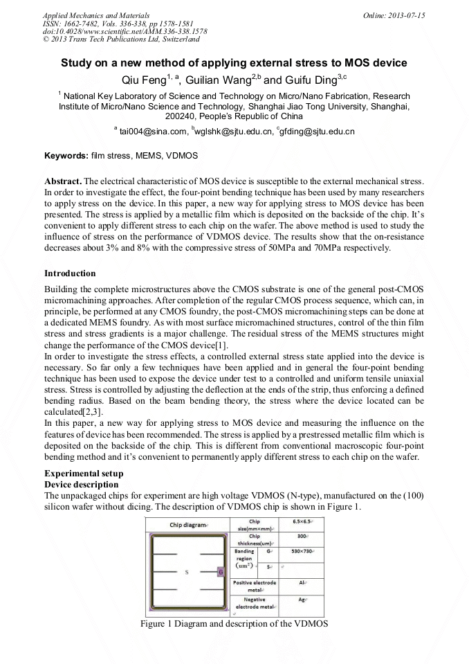
p.1578
p.1582
p.1587
p.1593
p.1597
Study on a New Method of Applying External Stress to MOS Device

Abstract:
The electrical characteristic of MOS device is susceptible to the external mechanical stress. In order to investigate the effect, the four-point bending technique has been used by many researchers to apply stress on the device. In this paper, a new way for applying stress to MOS device has been presented. The stress is applied by a metallic film which is deposited on the backside of the chip. Its convenient to apply different stress to each chip on the wafer. The above method is used to study the influence of stress on the performance of VDMOS device. The results show that the on-resistance decreases about 3% and 8% with the compressive stress of 50MPa and 70MPa respectively.
Info:
Periodical:
Pages:
1578-1581
Citation:
Online since:
July 2013
Authors:
Keywords:
Price:
Сopyright:
© 2013 Trans Tech Publications Ltd. All Rights Reserved
Share:
Citation: