Mechanism of Whisker Growth on Pure Sn Coating of Cu Leads in the High Temperature/Humidity Storage Tests

Article Preview

Abstract:

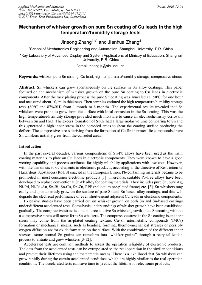
Sn whiskers can grow spontaneously on the surface in Sn alloy coatings. This paper focused on the mechanism of whisker growth on the pure Sn coating to Cu leads in electronic components. After the rack plating process the pure Sn coating was annealed at 150°C for one hour and measured about 10mm in thickness. Then samples endured the high temperature/humidity storage tests (60°C and 87%RH) from 1 month to 6 months. The experimental results revealed that Sn whiskers were prone to grow from the surface with local corrosion in the Sn coating. This was the high temperature/humidity storage provided much moisture to cause an electrochemistry corrosion between Sn and H2O. The excess formation of SnO2 had a large molar volume comparing to Sn and this generated a high inner stress in the corroded areas to shear the coating surface producing the defects. The compressive stress deriving from the formation of Cu-Sn intermetallic compounds drove Sn whiskers initially grew from the corroded areas.

You might also be interested in these eBooks

Info:

Periodical:

Pages:

2691-2695

Citation:

Online since:

December 2010

Export:

Price:

Permissions CCC:

Permissions PLS:

Сopyright:

© 2011 Trans Tech Publications Ltd. All Rights Reserved

Share:

Citation:

[1] Information on http: /www. netregs. gov. uk/ netregs/legislation/380525/ 477158.

Google Scholar

[2] M. Martin, D. Lea, J. Nottay and C. Hunt, in: NPL Report MATC (A47), (2001).

Google Scholar

[3] K.N. Tu: Physics Review B, Vol. 49 (1994), p. (2030).

Google Scholar

[4] B.Z. Lee and D.N. Lee: Acta Materialia Vol. 46 (1998), p.3701.

Google Scholar

[5] M. Dittes, P. Oberndorff and P. Petit, in: Proceedings of the 53rd Electronic Components and Technology Conference, New Orleans, LA, USA, May 2003, p.822.

Google Scholar

[6] G.T. Sheng, C.F. Hu, W.J. Choi, K.N. Tu, Y.Y. Bong and L. Nguyen: Journal of Applied Physics, Vol. 92 (2002), p.64.

Google Scholar

[7] M. Dittes, P. Oberndorff and P. Crema, in: Proceedings of the 5th Electronic Packaging Technology Conference, Singapore, December 2003, p.183.

Google Scholar

[8] W. J. Choi, T. Y. Lee, K. N. Tu and N. Tamura: Acta Materialia, Vol. 51 (2003), p.6253.

Google Scholar

[9] J. W. Osenbach, R. L. Shook, B. T. Vaccaro, B. D. Potteiger and A. Amin, in: Proceedings of the 54th Electronic Components and Technology Conference, Las Vegas, Nevada USA, June 2004, p.1314.

DOI: 10.1109/ectc.2004.1320283

Google Scholar

[10] G. T. Galyon and L. Palmer: IEEE Transactions on Electronics Packaging Manufacturing, Vol. 28 (2005), p.17.

Google Scholar

[11] C. Xu, Y. Zhang, C. Fan and J. Abys: IEEE Transactions on Electronics Packaging Manufacturing, Vol. 28 (2005), p.31.

Google Scholar

[12] K. S. Kim, C.H. Yu and J.M. Yang: Microelectronics Reliability, Vol. 46 (2006), p.1080.

Google Scholar

[13] R. Schetty, in: Proceedings of IPC Works 2000, pp: S-02-3-1.

Google Scholar

[14] K. Zeng and K.N. Tu: Materials Science and Engineering, Vol. 38 (2002), p.92.

Google Scholar

[15] J.W. Osenbach, J.M. DeLucca, B.D. Potteiger, R.L. Shook and F.A. Iaocchi, in: Proceedings of the 55th Electronic Components and Technology Conference, iNEMI Tin Workshop, Orlando, FL, USA, June 1, (2005).

Google Scholar