Thermal Effects Analysis of Flip Chip LED Packages with through Silicon via (TSV) by Using Numerical Simulation

Article Preview

Abstract:

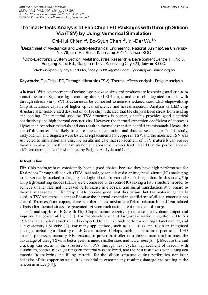
With advancement of technology, package sizes and products are becoming smaller due to miniaturization. Separate light-emitting diode (LED) chips and control integrated circuits with through silicon via (TSV) structurescan be combined to achieve reduced size. LED chipswithFlip Chip structureare capable of higher optical efficiency and heat dissipation. Analysis of LED chip structure after heat-related destruction of the chip indicated that the chip suffered stress from heating and cooling. The material used for TSV structures is copper, sincethis provides good electrical conductivity and high thermal conductivity. However, the thermal expansion coefficient of copper is higher than for other materials and can result in thermal expansion coefficient mismatch. Hence, the use of this material is likely to cause stress concentration and thus cause damage. In this study, molybdenum and tungsten were tested as replacements for copper in TSV, and the modified TSV was subjected to simulation analysis.The results indicate that replacement of TSV materials can reduce thermal expansion coefficient mismatch and consequent stress fracture and that the performance of different materials can be simulated by Fatigue Analysis and Load.

You might also be interested in these eBooks

Info:

Periodical:

Pages:

289-294

Citation:

Online since:

October 2013

Export:

Price:

Permissions CCC:

Permissions PLS:

Сopyright:

© 2014 Trans Tech Publications Ltd. All Rights Reserved

Share:

Citation:

* - Corresponding Author

[1] Shao-Hua Huang, Ray-Hua Horng, Kuo-Sheng Wen, Yi-Feng Lin, Kuo-Wei Yen and Dong-Sing Wuu, Improved Light Extraction of Nitride-Based Flip-Chip Light-Emitting Diodes Via Sapphire Shaping and Texturing, IEEE PHOTONICS TECHNOLOGY LETTERS, Vol. 18, (2006).

DOI: 10.1109/lpt.2006.886823

Google Scholar

[2] Makoto Motoyoshi, Through-Silicon Via (TSV), Proceedings of the IEEE, Vol. 97, (2009), pp.43-48.

Google Scholar

[3] John Lau, Ricky Lee, Matthew Yuen and Philip Chan, 3D LED and IC wafer level packaging, Microelectronics International, Vol. 27, (2010), pp.98-105.

DOI: 10.1108/13565361011034786

Google Scholar

[4] XuejunFan, Wafer Level System Packaging and Integration for Solid State Lighting (SSL), IEEE 13th International Conference on Thermal, Mechanical and Multi-Physics Simulation and Experiments in Microelectronics and Microsystems, (2012).

DOI: 10.1109/esime.2012.6191771

Google Scholar

[5] Kuan H. Lu, Suk-Kyu Ryu, Qiu Zhao, Xuefeng Zhang, Jay Im, Rui Huang and Paul S. Ho, Thermal Stress Induced Delamination of Through Silicon Vias in 3-D Interconnects, IEEE Electronic Components and Technology Conference, (2010), pp.40-45.

DOI: 10.1109/ectc.2010.5490883

Google Scholar

[6] Juergen Auersperg, Dietmar Vogel, Ellen Auerswald, Sven Rzepka and Bernd Michel, Nonlinear Copper Behavior of TSV for 3D-IC-Integration and Cracking Risks during BEoL-Built-up, IEEE 13th Electronics Packaging Technology Conference, (2011).

DOI: 10.1109/eptc.2011.6184380

Google Scholar

[7] Zhimin Wan, Xiaobing Luo and Sheng Liu, Effect of Blind Hole Depth and Shape of Solder Joint on the Reliability of Through Silicon Via (TSV), IEEE Electronic Components and Technology Conference, (2011), pp.1657-1661.

DOI: 10.1109/ectc.2011.5898734

Google Scholar

[8] Suk-Kyu Ryu, Kuan-Hsun Lu, Tengfei Jiang, Jang-Hi Im, Rui Huang and Paul S. Ho, Effect of Thermal Stresses on Carrier Mobility and Keep-Out Zone Around Through-Silicon Vias for 3-D Integration, IEEE Transactions on Device and Materials Reliability, Vol. 12, (2012).

DOI: 10.1109/tdmr.2012.2194784

Google Scholar

[9] Bahareh Banijamali, Suresh Ramalingam, Kumar Nagarajan and Raghu Chaware, Advanced Reliability Study of TSV Interposers and Interconnects for the 28nm Technology FPGA, IEEE Electronic Components and Technology Conference, (2011), pp.285-290.

DOI: 10.1109/ectc.2011.5898527

Google Scholar