p.1416
p.1423
p.1427
p.1431
p.1436
p.1441
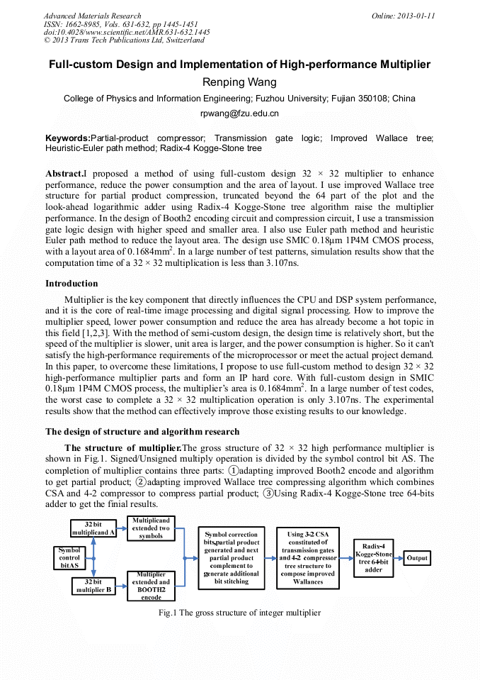
p.1445
p.1452
p.1457
Full-Custom Design and Implementation of High-Performance Multiplier

Abstract:
I proposed a method of using full-custom design 32 × 32 multiplier to enhance performance, reduce the power consumption and the area of layout. I use improved Wallace tree structure for partial product compression, truncated beyond the 64 part of the plot and the look-ahead logarithmic adder using Radix-4 Kogge-Stone tree algorithm raise the multiplier performance. In the design of Booth2 encoding circuit and compression circuit, I use a transmission gate logic design with higher speed and smaller area. I also use Euler path method and heuristic Euler path method to reduce the layout area. The design use SMIC 0.18μm 1P4M CMOS process, with a layout area of 0.1684mm2. In a large number of test patterns, simulation results show that the computation time of a 32 × 32 multiplication is less than 3.107ns.
Info:
Periodical:
Pages:
1445-1451
Citation:
Online since:
January 2013
Authors:
Price:
Сopyright:
© 2013 Trans Tech Publications Ltd. All Rights Reserved
Share:
Citation: