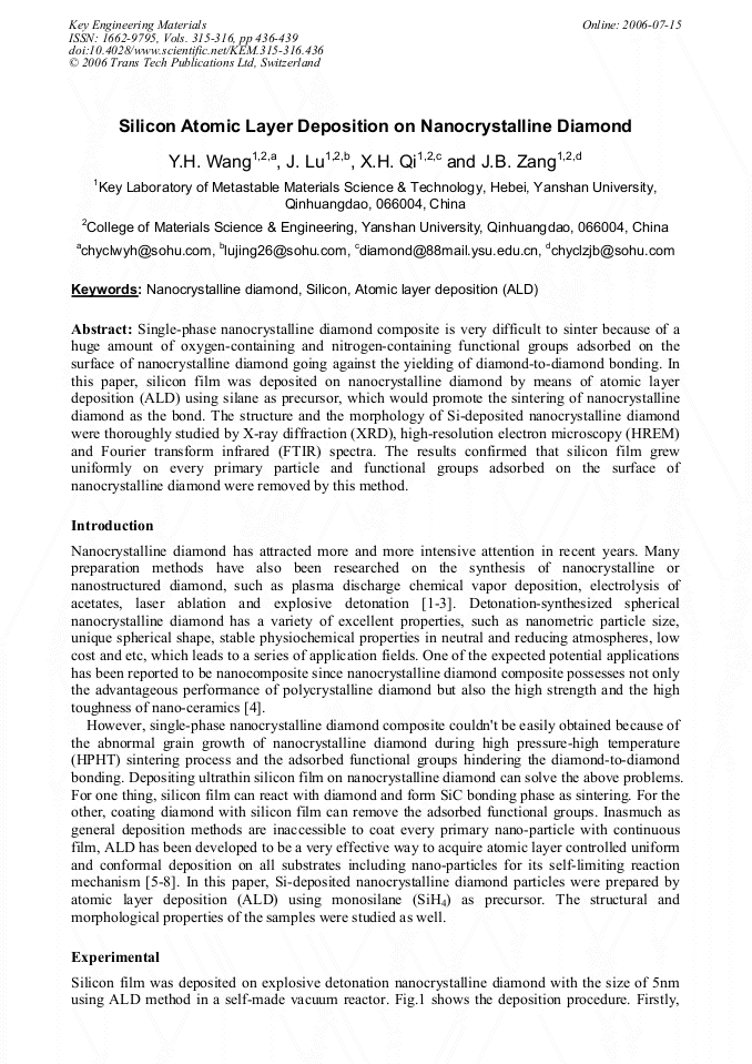
Silicon Atomic Layer Deposition on Nanocrystalline Diamond

Article Preview

Abstract:

Single-phase nanocrystalline diamond composite is very difficult to sinter because of a huge amount of oxygen-containing and nitrogen-containing functional groups adsorbed on the surface of nanocrystalline diamond going against the yielding of diamond-to-diamond bonding. In this paper, silicon film was deposited on nanocrystalline diamond by means of atomic layer deposition (ALD) using silane as precursor, which would promote the sintering of nanocrystalline diamond as the bond. The structure and the morphology of Si-deposited nanocrystalline diamond were thoroughly studied by X-ray diffraction (XRD), high-resolution electron microscopy (HREM) and Fourier transform infrared (FTIR) spectra. The results confirmed that silicon film grew uniformly on every primary particle and functional groups adsorbed on the surface of nanocrystalline diamond were removed by this method.

You might also be interested in these eBooks

Info:

Periodical:

Key Engineering Materials (Volumes 315-316)

Pages:

436-439

Citation:

Online since:

July 2006

Export:

Price:

Permissions CCC:

Permissions PLS:

Сopyright:

© 2006 Trans Tech Publications Ltd. All Rights Reserved

Share:

Citation:

[1] P. Aublanc, V.P. Novikov, L.V. Kuznetsova and M. Mermoux: Diamond and Related Materials, Vol. 10 (2001), pp.942-946.

DOI: 10.1016/s0925-9635(00)00548-3

Google Scholar

[2] S.R.J. Pearce, S.J. Henley, F. Claeyssens, P.W. May, K.R. Hallam, J.A. Smith and K.N. Rosser: Diamond and Related Materials, Vol. 13 (2004), pp.661-665.

DOI: 10.1016/j.diamond.2003.08.027

Google Scholar

[3] P.W. Chen, Y.S. Ding, Q. Chen, F.L. Huang and S.R. Yun: Diamond and Related Materials Vol. 9 (2000), pp.1722-1725.

Google Scholar

[4] G.A. Voronin, T.W. Zerda, J. Qian, Y. Zhao, D. He and S.N. Dub: Diamond and Related Materials, Vol. 12 (2003), pp.1477-1481.

Google Scholar

[5] J.W. Klaus and S.M. George: Surface Science, Vol. 447 (2000), pp.81-90.

Google Scholar

[6] B. Min, J.S. Lee, J.W. Hwang, K.H. Keem, M.I. Kang, K. Cho, M.Y. Sung, S. Kim, M.S. Lee, S.O. Park and J.T. Moon: Journal of Crystal Growth, Vol. 252 (2003), pp.565-569.

DOI: 10.1016/s0022-0248(03)00967-9

Google Scholar

[7] D.M. Hausman, P.D. Rouffignac, A. Smith, R. Gordon and D. Monsma: Thin Solid Films, Vol. 443 (2003), pp.1-4.

Google Scholar

[8] A.M. Lemonds, J.M. White and J.G. Ekerdt: Surface Science, Vol. 538 (2003), pp.191-203.

Google Scholar