Analysis of Electroluminescence Application on Display

Article Preview

Abstract:

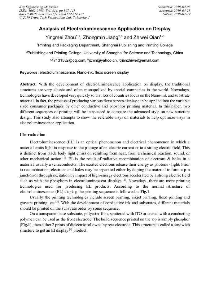
With the development of electroluminescence application on display, the traditional structures are very classic and often monopolized by special companies in the world. Nowadays, technologies have developed very quickly so that lots of countries focus on the nanoink and substrate material. In fact, the process of producing various flexo screen display can be applied into the variable sized consumer packages by other conductive and phosphor printing material. In this paper, two different sequences of printing will be introduced to compare the advanced style on new structure design. This study also attempts to show the referable ways on materials to help optimize ways in electroluminescence application.

You might also be interested in these eBooks

Info:

Periodical:

Pages:

107-111

Citation:

Online since:

July 2019

Export:

Price:

Permissions CCC:

Permissions PLS:

Сopyright:

© 2019 Trans Tech Publications Ltd. All Rights Reserved

Share:

Citation:

* - Corresponding Author

[1] Raguse, John (April 15, 2015). Correlation of Electroluminescence with Open-Circuit Voltage from Thin-Film CdTe Solar Cells,. Journal of Photovoltaics. 5(4): 1175–1178.

DOI: 10.1109/JPHOTOV.2015.2417761

Google Scholar

[2] Wu Y L, Li Y N,Ong BS. A simple and efficient approach to a printable silver conductor for printed electronics [J]. Journal of the American Chemical Society, 2007, 129(7):1862.

DOI: 10.1021/ja067596w

Google Scholar

[3] Yuan Xiaofeng, Micro-structure Patterning Technology & its Application in Printed Electronics[D], (2009).

Google Scholar

[4] C. Michael Shedd,Variability of Electroluminescent Displays,(2011).

Google Scholar

[5] Z.Yingmei, J.Zhongmin, Analysis on Printed Electronics Circuit Design, NIP32 ,(2017).

Google Scholar

[6] Roger Bollström, Impact of humidity on functionality of on-paper printed electronics, Nanotechnology 25, (2014).

Google Scholar

[7] Veronica Kopp . Design and Production Aspects of an Electroluminescent Segment Display; Nov (2012).

Google Scholar

[8] Xiaoying Rong,Characterize Screen Printing Parameters for Electroluminescent Inks. California Polytechnic State University (2010).

Google Scholar

[9] Zeng Y, Ning HL, Zheng K,etal. A room temperature strategy towards enhanced performance and bias stability of oxide thin film transistor with a sandwich structures channel layer [J]. Applied physics Letters, 2017, 110(15):153503.

DOI: 10.1063/1.4979868

Google Scholar

[10] Vivek Subramanian,Printed Electronics For Low-Cost Electronic Systems: Technology Status and Application Development,China Printing And tudy Vol.01 No.03 (2009).

Google Scholar

[11] M.R. Chaharmir, Reflectarray design using printed electronics Technology,Electronics Letters 25th October (2012 )Vol. 48 No. 22.

DOI: 10.1049/el.2012.3329

Google Scholar

[12] Cai jiqing. Development of conductive nano ink material for printed electronics,Printing Circus Information, (2015).

Google Scholar