Electrical Resistivity and Application of Cu3N Thin Films
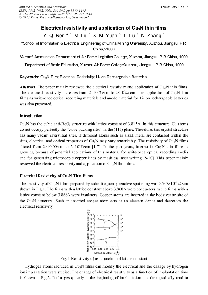
Article Preview

Abstract:

The paper mainly reviewed the electrical resistivity and application of Cu3N thin films. The electrical resistivity increases from 2×10⁻⁵Ω•cm to 2×10²Ω•cm. The application of Cu3N thin films as write-once optical recording materials and anode material for Li-ion rechargeable batteries was also presented.

You might also be interested in these eBooks

Info:

Periodical:

Pages:

1140-1143

Citation:

Online since:

December 2012

Export:

Price:

Permissions CCC:

Permissions PLS:

Сopyright:

© 2013 Trans Tech Publications Ltd. All Rights Reserved

Share:

Citation:

[1] T. Maruyama, T. Morishita, Copper nitride thin films prepared by redio-frequency reactive sputtering, J. Appl. Phys., 1995; 78 (6): 4104.

DOI: 10.1063/1.359868

Google Scholar

[2] Y. Hayashi , T. Ishikawa, D. Shimokawa, Modification of electrical and optical properties of metal nitride thin films by hydrogen inclusion, Journal of Alloys and Compounds, 2002; 330-332: 348 –351.

DOI: 10.1016/s0925-8388(01)01495-5

Google Scholar

[3] J. F. Pierson, Structure and properties of copper nitride films formed by reactive magnetron sputtering, Vacuum 2002; 66: 59-64.

DOI: 10.1016/s0042-207x(01)00425-0

Google Scholar

[4] D. Écija, et al. The adsorption of atomic N and the growth of copper nitrides on Cu (100). Surface Science 2009; 603: 2283–2289.

DOI: 10.1016/j.susc.2009.04.039

Google Scholar

[5] T. Nosaka, M. Yoshitake, A. Okamoto, et al. Copper nitride thin films prepared by reactive radio-frequency magnetron sputtering, Thin Solid Films 1999; 348: 8-13.

DOI: 10.1016/s0040-6090(98)01776-3

Google Scholar

[6] D. M. Borsa, and D. O. Boerma, Growth, structure and optical properties of Cu3N films, Surface Science 2004; 548: 95.

DOI: 10.1016/j.susc.2003.10.053

Google Scholar

[7] S. Terada, H. Tanaka, Kubota K. Heteroepitaxial growth of Cu3N thin films, J. Cryst. Growth, 1989; 94: 567~568.

DOI: 10.1016/0022-0248(89)90038-9

Google Scholar

[8] T. Maruyama, T. Morishita, Copper nitride and tin thin films for write-once optical recording media, Appl. Phys. Lett., 1996; 69 (7): 890~891.

DOI: 10.1063/1.117978

Google Scholar

[9] M. Asano, K. Umeda, Tasaki A. Cu3N thin film for a new light recording media[J]. Jpn. J. Appl. Phys., 1990; 29 (10): 1985~(1986).

DOI: 10.1143/jjap.29.1985

Google Scholar

[10] K. J. Kim, J. H. Kim, J. H. Kang, Structural and optical characterization of Cu3N films prepared by reactive RF magnetron sputtering, J. Cryst. Growth, 2001 222: 767.

DOI: 10.1016/s0022-0248(00)00968-4

Google Scholar

[11] T. Nosaka, M. Yoshitake, A. Okamoto, et al. Thermal decomposition of copper nitride thin films and dots formation by electron bean writing, Appl. Surf. Sci., 2001 169-170: 358.

DOI: 10.1016/s0169-4332(00)00681-4

Google Scholar

[12] Z. Liu, F. Wu, Anode material of copper nitride thin film for Li-ion rechargeable batteries, Electrical Source Technology, 2008. 3: 154.

Google Scholar