p.1341
p.1345
p.1349
p.1353
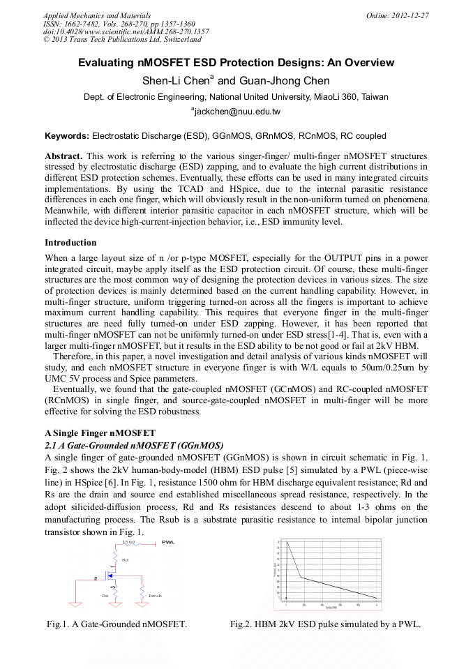
p.1357
p.1361
p.1367
p.1371
p.1376
Evaluating nMOSFET ESD Protection Designs: An Overview

Abstract:
This work is referring to the various singer-finger/ multi-finger nMOSFET structures stressed by electrostatic discharge (ESD) zapping, and to evaluate the high current distributions in different ESD protection schemes. Eventually, these efforts can be used in many integrated circuits implementations. By using the TCAD and HSpice, due to the internal parasitic resistance differences in each one finger, which will obviously result in the non-uniform turned on phenomena. Meanwhile, with different interior parasitic capacitor in each nMOSFET structure, which will be inflected the device high-current-injection behavior, i.e., ESD immunity level.
Info:
Periodical:
Pages:
1357-1360
Citation:
Online since:
December 2012
Authors:
Keywords:
Price:
Сopyright:
© 2013 Trans Tech Publications Ltd. All Rights Reserved
Share:
Citation: