[4]
. The surface morphology of thin films will change depending with different stack sequence in precursors.
Google Scholar
[5]
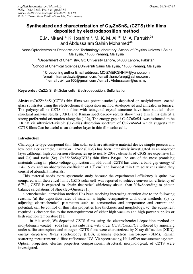
Fig. 1. Surface SEM image of the CZTS thin film. The crystal structures of the as-synthesized CZTS nanostructures were characterized by X-ray diffraction XRD measurements. Fig. 2 shows the XRD patterns of the as-synthesized CZTS nanoparticles deposited by electrochemical deposition with 2θ scanning from 20° to 80o. XRD measurement show peaks are attributable to Cu2ZnSnS4 were (112), (220), (132), (224) , (332). the film observed to be grown well with good crystallinity. The phase show pointed to the presence of CZTS with the kieserite Structure with preferred orientation along the (1 1 2) plane which are in agreement with the previous reports(6, 7) . some metal sulfide and other secondary phases were also appear as SnS was present at (130). Molybdenum back contact appear at (110). also XRD pattern shows sharp peaks that indicate good crystall Fig. 2. XRD pattern of as-synthesized annealed Cu2CdSnS4 XRD does not allow the distinction between the CZTS and ZnS, for that Raman was performed to characterize the samples, Raman spectrum of the resulting sample (Fig. 3) shows a main peak at 338 cm−1 quality and Secondary peaks at 288 and 368 cm−1 attributed to the CZTS structure for higher Cu/ (Zn+Sn) elemental ratios at Cu/ (Zn+Sn) =0. 81. The Raman spectra of the as-synthesized CZTS microparticles show that the most intense peak is located at 338 cm−1which indicating that the as-synthesized products are the CZTS thin film. There is no peak at 351 cm −1and 274 cm−1 attributed to ZnS which overlap. Full width at half maximum (FWHM) for 338 cm−1 peak is 7. 8 cm−1. Moreover, the strong major and sharp peak is the indication of good crystalline (8). Fig. 3. Raman spectrum of CZTS thin film. Optical properties The band gap energy was derived from the plot of (αhv)2 with hv. Where α is the absorption coefficient. The hv is the photon energy. Determine the absorption coefficient we use the thickness of the films and measured spectral transmittance and reflectance using a UV–vis–NIR. Fig. 4 shows (αhv)2 with hv plot for the CZTS films sulfurized for 2 h in S atmospheres . The band gaps of the CZTS thin film was1. 8eV, These band gaps are close to the optimum value for a photovoltaic solar cell, and also near to the results reported by other research groups( 5, 6, 7). Annealing duration increases and the annealing temperature will increases the band gap value.
Google Scholar
[8]
The optical and electrical properties which mainly depend on composition and crystal of the absorber material structure, effect on the performance of the solar cell. The CZTS surfaces were examined using atomic force microscopy (AFM). The AFM images of CZTS on molybdenum coated glass typically showed a good coverage of CZTS (Figure 5). The AFM images showed more elongated particles and show the smooth, uniform, homogeneous and densely packed grains. The conductivity type detected by a Hall effect measurements is a p-type semiconductor with , With a carrier concentration of 4. 00×1014 cm–2 , a sheet resistance of 1. 6×10 -2 Ω/square, a Hall mobility of approximately1. 47×10 6 cm2/V-Sec, and a Hall coefficient of 1. 56 m2/C . poor crystallinity and small particles size affect in high resistivity[ 9]. In CZTS , the resistivity was varied depending on the ratio of Cu/(Zn + Sn) , for that copper has important role in determining the resistivity of films rather than other metals.
Google Scholar
[10]
. Fig4. Plots of (αhv) vs. hv for Cu2ZnSnS4 thin film. Fig. 5. AFM image of Cu2ZnSnS4 thin film. Conclusions In conclusion, we have successfully synthesized kesterite Cu2ZnSnS4 (CZTS) thin films by electrochemical deposition method on molybdenum coated soda lim glass substrate. the synthesized CZTS thin films were characterized by various techniques like , Raman spectroscopy, UV–vis spectroscopy, X-ray diffraction, Hall effect measurements . optical, structural, compositional, and electrical properties of the prepared CZTS thin films have been characterized . The optical absorption study shows the a band gap energy of 1. 8 eV. And XRD indicate presence of CZTS with the kesterite Structure in preferred orientation along the (1 1 2) plane. Hall Effect shows the high carrier concentration with low resistivity. Acknowledgements This work was supported by the Nano-optoelectronics Research Laboratory, School of Physics: UniversitiSains Malaysia under grant number 203/PSF-6721001 and TWAS. Refrence.
Google Scholar
[1]
W. Shockley and H.J. Queisser, J. Appl. Phys. Vol. 32 (1961) , p.510–519.
Google Scholar
[2]
J. Lee, S. C. Nam and Y. Tak, Korean J. Chem. Eng, Vol. 22 (2005) , pp.161-164.
Google Scholar
[3]
A. Wangperawong, J.S. King , S.M. Herron, B.P. Tran, K. Pangan and S.F. Bent, Thin Solid Films Vol. 519 (2011) , p.2488–2492.
DOI: 10.1016/j.tsf.2010.11.040
Google Scholar
[4]
T. Tanaka, D. Kawasaki, M. Nishio, Q. Guo and H. Ogawa, Phys. Status Solidi (c) Vol. 3 (2006) , p.2844–2847.
Google Scholar
[5]
H. Araki, A. Mikaduki, Y. Kubo, T. Sato, K. Jimbo, W.S. Maw, H. Katagiri, M. Yamazaki, K. Oishi and A. Takeuchi, Thin Solid Films Vol. 517 (2008) , p.1457–1460.
DOI: 10.1016/j.tsf.2008.09.058
Google Scholar
[5]
K. Maeda , K. Tanaka, Y. Nakano, Y. Fukui, and H. Uchiki - Jpn. J. Appl. Phys. Vol. 50 (2011) , pp.05-09.
Google Scholar
[6]
H. Katagiri, N. Ishigaki, T. Ishida and K. Saito, Japanese Journal of Applied Physics Vol. 40 (2001) , p.500–504.
Google Scholar
[7]
Y. Shi, Z.G. Jin, C.Y. Li, H.S. An and J.J. Qiu, Applied Surface Science Vol. 252 (2006) , p.3737–3743.
Google Scholar
[8]
V. Kheraj , K.K. Patel, S.J. Patel and D.V. Shah - Journal of Crystal Growth Vol. 362, 1 (2013) , p.174–177.
Google Scholar
[9]
H. Katagiri, N. Ishigaki, T. Ishida and K. Saito, Japanese Journal of Applied Physics Vol. 40 (2001), p.500–504.
Google Scholar
[10]
H. Katagiri, N. Ishigaki, T. Ishida and K. Saito, Japanese Journal of Applied Physics Vol. 40 (2001), p.500–504.
Google Scholar