Microstructure and Electrical Properties of Lead-Free (Na0.5K0.5)NbO3 - Bi0.5(Na0.97K0.03)0.5TiO3 Ceramics

Article Preview

Abstract:

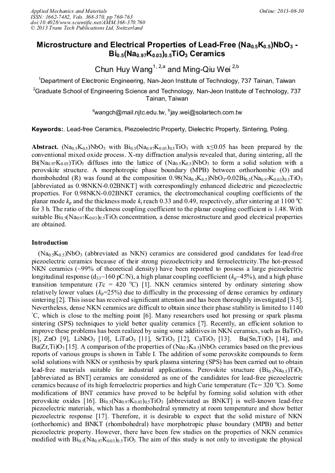
(Na0.5K0.5)NbO3 with Bi0.5(Na0.97K0.03)0.5TiO3 with x≤0.05 has been prepared by the conventional mixed oxide process. X-ray diffraction analysis revealed that, during sintering, all the Bi(Na0.97K0.03)TiO3 diffuses into the lattice of (Na0.5K0.5)NbO3 to form a solid solution with a perovskite structure. A morphotropic phase boundary (MPB) between orthorhombic (O) and rhombohedral (R) was found at the composition 0.98(Na0.5K0.5)NbO3-0.02Bi0.5(Na0.97K0.03)0.5TiO3 [abbreviated as 0.98NKN-0.02BNKT] with correspondingly enhanced dielectric and piezoelectric properties. For 0.98NKN-0.02BNKT ceramics, the electromechanical coupling coefficients of the planar mode kp and the thickness mode kt reach 0.33 and 0.49, respectively, after sintering at 1100 oC for 3 h. The ratio of the thickness coupling coefficient to the planar coupling coefficient is 1.48. With suitable Bi0.5(Na0.97K0.03)0.5TiO3 concentration, a dense microstructure and good electrical properties are obtained.

You might also be interested in these eBooks

Info:

Periodical:

Pages:

760-763

Citation:

Online since:

August 2013

Export:

Price:

Permissions CCC:

Permissions PLS:

Сopyright:

© 2013 Trans Tech Publications Ltd. All Rights Reserved

Share:

Citation:

[1] G. Shirane, R. Newnham, and R. Pepinsky: Phys. Rev. Vol. 96 (1954), p.581.

Google Scholar

[2] M. D. Maeder, D. Damjanovic, and N. Setter: J. Electroceram. Vol. 13 (2004), p.385.

Google Scholar

[3] V. Lingwal, B. S. Semwal, and N. S. Panwar: Bull. Mater. Sci. Vol. 26 (2003), p.619.

Google Scholar

[4] H. Birol, D. Damjanovic, and N. Setter: J. Eur. Ceram. Soc. Vol. 26 (2006), p.861.

Google Scholar

[5] T. Takenaka, H. Nagata, and Y. Hiruma: Jpn. J. Appl. Phys. Vol. 47 (2008), p.3787.

Google Scholar

[6] S. Y. Chu, W. Water, Y. D. Juang, J. T. Liaw, and S. B. Dai: Ferroelectrics Vol. 297 (2003), p.11.

Google Scholar

[7] M. Matsubara,T. Yamaguchi, K. Kikuta, and S. Hirano: Jpn. J. Appl. Phys. Vol. 44 (2005), p.6136.

Google Scholar

[8] S. H. Park, C. W. Ahn, S. Nahm, and J. S. Song: Jpn. J. Appl. Phys. Vol. 43 (2004), p. L1072.

Google Scholar

[9] Y. Guo, K. Kakimoto, and H. Ohsato: Jpn. J. Appl. Phys. Vol. 43 (2004), p.6662.

Google Scholar

[10] Y. Guo, K. Kakimoto, and H. Ohsato: Appl. Phys. Lett. Vol. 85 (2004), p.4121.

Google Scholar

[11] Y. Guo, K. Kakimoto, and H. Ohsato: Mater. Lett. Vol. 59 (2005), p.241.

Google Scholar

[12] M. Kosec, V. Bobnar, M. Hrovat, J. Bernard, and J. Holc: J. Mater. Res. Vol. 19 (2004), p.1849.

Google Scholar

[13] R. C. Chang, S. Y. Chu, Y. F. Lin, and, P. C. Kao: Sens. Actuators A Vol. 138 (2007), p.355.

Google Scholar

[14] C. H. Wang: J. Ceram. Soc. Jpn. Vol. 117.

Google Scholar

[5] (2009), p.680.

Google Scholar

[15] C. H. Wang: Japanese Jpn. J. Appl. Phys. Vol. 48 (2009), p.041403.

Google Scholar

[16] )]C. H. Wang: J. Ceram. Soc. Jpn. Vol. 116 (2008), p.632.

Google Scholar

[17] C. H. Wang: Advanced Materials Research Vol. 239-242 (2011), p.3240.

Google Scholar