Barrier and Seed Layers Deposition in TSV Using Magnetron Sputtering

Article Preview

Abstract:

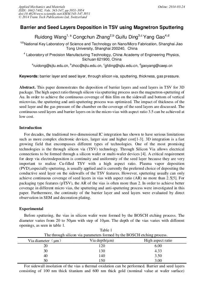
This paper demonstrates the deposition of barrier layers and seed layers in TSV for 3D package. The high aspect ratio through silicon via sputtering process uses the magnetron-sputtering of Au. In order to achieve the continuous coverage of thin film on the sidewall and bottom of vertical microvias, the sputtering and anti-sputtering process was optimized. The impact of thickness of the seed layer and the gas pressure of the chamber on the coverage of the seed layers are discussed. The continuous seed layers and barrier layers on in the micro-vias with aspect ratio 3.5 can be achieved at low cost.

You might also be interested in these eBooks

Info:

Periodical:

Pages:

3951-3954

Citation:

Online since:

March 2014

Export:

Price:

Permissions CCC:

Permissions PLS:

Сopyright:

© 2014 Trans Tech Publications Ltd. All Rights Reserved

Share:

Citation:

* - Corresponding Author

[1] R. Beica, P. Siblerud, in: High-Speed Cu-TSV for 5: 1 iTSV Applications, ECS Transactions, 18 (2009) , 689-694.

DOI: 10.1149/1.3096522

Google Scholar

[2] Tsui K.Y. K, Yau S.K., Leung V.C.K., in: Parametric study of electroplating-based via-filling process for tsv applications, 2009 International Conference on Electronic Packaging Technology & High Density Packaging(2009), 23-27.

DOI: 10.1109/icept.2009.5270801

Google Scholar

[3] Wolf M.J., Dretschkow T., Wunderle B., Jurgensen N., Engelmann G., Ehrmann O., Uhlig, A., Michel B., Reichl H., in: High aspect ratio TSV copper filling with different seed layers, 58th Electronic Components and Technology Conference(2008).

DOI: 10.1109/ectc.2008.4550029

Google Scholar

[4] Information on http: /www. micralyne. com/through-silicon-via.

Google Scholar

[5] Mai SL,  Zhu YH, Sun X , Miao M, Chen J, Jin YF, in: Fabrication and in-situ evaluation of Copper TSV Interconnection, 12th International Conference on Electronic Packaging Technology and High Density Packaging(2011), 114-117.

DOI: 10.1109/icept.2011.6066801

Google Scholar

[6] O. Lühn C. Van Hoof, W. Ruythooren, J. -P. Celis, in: Barrier and seed layer coverage in 3D structures with different aspect ratios using sputtering and ALD processes, Microelectronic Engineering, 85 (2008) 1947–(1951).

DOI: 10.1016/j.mee.2008.06.007

Google Scholar