Controlling the Growth of ZnO-SiO2 Nanostructures Using Pt-Coated Si Substrate

Article Preview

Abstract:

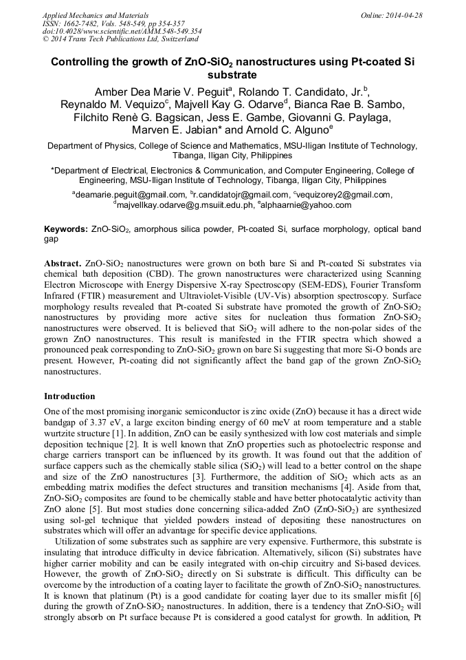
ZnO-SiO2 nanostructures were grown on both bare Si and Pt-coated Si substrates via chemical bath deposition (CBD). The grown nanostructures were characterized using Scanning Electron Microscope with Energy Dispersive X-ray Spectroscopy (SEM-EDS), Fourier Transform Infrared (FTIR) measurement and Ultraviolet-Visible (UV-Vis) absorption spectroscopy. Surface morphology results revealed that Pt-coated Si substrate have promoted the growth of ZnO-SiO2 nanostructures by providing more active sites for nucleation thus formation ZnO-SiO2 nanostructures were observed. It is believed that SiO2 will adhere to the non-polar sides of the grown ZnO nanostructures. This result is manifested in the FTIR spectra which showed a pronounced peak corresponding to ZnO-SiO2 grown on bare Si suggesting that more Si-O bonds are present. However, Pt-coating did not significantly affect the band gap of the grown ZnO-SiO2 nanostructures.

You might also be interested in these eBooks

Info:

* - Corresponding Author

[1] N.K. Hassan, M.R. Hashim, M.A. Mahdi and N.K. Allam: ECS Journal of Solid State Science and Technology Vol. 1 (2012), pp.86-89.

Google Scholar

[2] C.D. Lokhande, P.M. Gondkar, R. Mane, V.R. Shinde and S.H. Han: Journal of Alloys and Compounds Vol. 475 (2009), pp.304-311.

DOI: 10.1016/j.jallcom.2008.07.025

Google Scholar

[3] A. Laurentowska and T. Jesionowski: Physiocochem. Probl. Miner. Process Vol. 48 (2012), pp.63-76.

Google Scholar

[4] Y. Yang, Y.Q. Li, H.Q. Shi, W.N. Li, H.M. Xiao, L.P. Zhu, Y.S. Luo, S.Y. Fu and T. Liu: Composites: Part B Vol. 42 (2011), pp.2105-2110.

Google Scholar

[5] R. Hong, T. Pan, J. Qian and H. Li: Chemical Engineering Journal Vol. 119 (2006), pp.71-81.

Google Scholar

[6] H. Yamada, Y. Ushimi, M. Takeuchi, Y. Yoshino, Makino T and Arai S: Vacuum Vol. 74 (2004), pp.689-692.

Google Scholar

[7] J.R. Duclère, C. McLoughlin, J. Fryar, R. O'Haire, M. Guilloux-Viry, A. Meaney, A. Perrin, E. McGlynn, M.O. Henry and J.P. Mosnier: Thin Solid Films Vol. 500 (2006), pp.78-83.

DOI: 10.1016/j.tsf.2005.11.017

Google Scholar

[8] M. Bakar, M. Hamid and A. Jalar: Advanced Research Materials Vol. 97-101 (2010), pp.1550-1553.

Google Scholar

[9] A. Sugunan, H.C. Warad, M. Boman and J. Dutta: J. Sol-Gel Sci Techn Vol. 39 (2006), pp.49-56.

Google Scholar

[10] K.V. Gurav, U.M. Patil, S.M. Pawar, J.H. Kim and C.D. Lokhande: Journal of Alloys and Compounds Vol. 509 (2011), pp.7723-7728.

DOI: 10.1016/j.jallcom.2011.04.094

Google Scholar