p.587
p.592
p.597
p.604
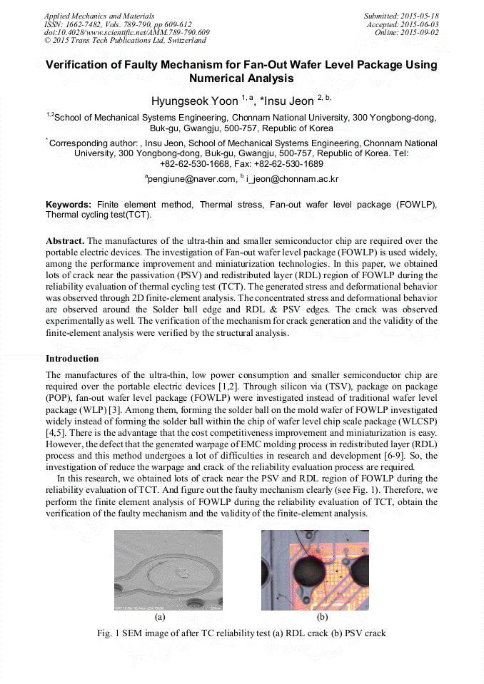
p.609
p.615
p.621
p.626
p.636
Verification of Faulty Mechanism for Fan-Out Wafer Level Package Using Numerical Analysis

Abstract:
The manufactures of the ultra-thin and smaller semiconductor chip are required over the portable electric devices. The investigation of Fan-out wafer level package (FOWLP) is used widely, among the performance improvement and miniaturization technologies. In this paper, we obtained lots of crack near the passivation (PSV) and redistributed layer (RDL) region of FOWLP during the reliability evaluation of thermal cycling test (TCT). The generated stress and deformational behavior was observed through 2D finite-element analysis. The concentrated stress and deformational behavior are observed around the Solder ball edge and RDL & PSV edges. The crack was observed experimentally as well. The verification of the mechanism for crack generation and the validity of the finite-element analysis were verified by the structural analysis.
Info:
Periodical:
Pages:
609-612
Citation:
Online since:
September 2015
Authors:
Price:
Сopyright:
© 2015 Trans Tech Publications Ltd. All Rights Reserved
Share:
Citation: