p.148
p.153
p.158
p.163
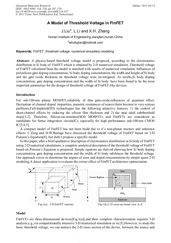
p.167
p.171
p.176
p.181
p.188
A Model of Threshold Voltage in FinFET

Abstract:
A physics-based threshold voltage model is proposed, according to the electrostatics distribution in Si body of FinFET which is obtained by 2-D numerical simulation. Threshold voltage of FinFET calculated from the model is matched with results of numerical simulation. Influences of polysilicon gate doping concentration, Si body doping concentration, the width and height of Si body and the gate oxide thickness on threshold voltage were investigated. As results,Si body doping concentration, gate doping concentration and the width of Si body have been found to be the most important parameters for the design of threshold voltage of FinFET-like devices.
Info:
Periodical:
Pages:
167-170
DOI:
Citation:
Online since:
March 2011
Authors:
Keywords:
Price:
Сopyright:
© 2011 Trans Tech Publications Ltd. All Rights Reserved
Share:
Citation: