p.2454
p.2458
p.2464
p.2469
p.2474
p.2478
p.2482
p.2486
p.2491
Probing Active-Area Shift with Improved Kelvin Measurement for Trench DRAM

Abstract:
In nano-like or nano-regime trench DRAM products, the product yield usually determines the marketing competition. Due to active area (AA) layer shift in lithography process, the cell leakage and the contact resistance at the source terminal of a cell transistor are increased. These factors will deteriorate the cell integrity in charging and access functions. To monitor this inferiority from lithography deviation, an improved Kelvin measurement and a novel pattern design were recommended. The yield improvement with this technology was really conspicuous.

Info:
Periodical:
Pages:
2474-2477
Citation:
Online since:
August 2011
Authors:
Keywords:
Price:
Сopyright:
© 2011 Trans Tech Publications Ltd. All Rights Reserved
Share:
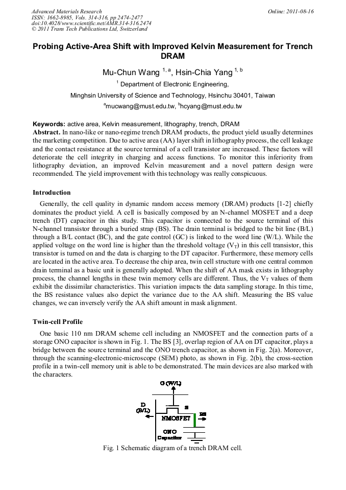
Citation: