p.1297
p.1301
p.1305
p.1309
p.1313
p.1317
p.1322
p.1326
p.1331
A Method of MEMS Package Using Local Laser Bonding
Abstract:
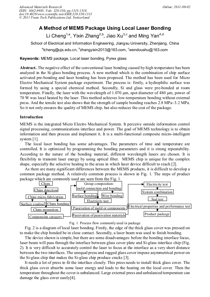
The negative effect of the conventional laser bonding caused by high temperature has been analyzed in the Si-glass bonding process. A new method which is the combination of chip surface activated pre-bonding and laser bonding has been proposed. The method has been used for Micro Electro Mechanical System package experiment. The process is: firstly, a hydrophilic surface was formed by using a special chemical method. Secondly, Si and glass were pre-bonded at room temperature. Finally, the laser with the wavelength of 1.070 μm, spot diameter of 480 μm, power of 70 W was local heated by the laser. This method achieves low-temperature bonding without external press. And the tensile test also shows that the strength of sample bonding reaches 2.8 MPa~3.2 MPa. So it not only ensures the quality of MEMS chip, but also reduces the cost of the package.
Info:
Periodical:
Pages:
1313-1316
Citation:
Online since:
September 2011
Authors:
Keywords:
Price:
Сopyright:
© 2011 Trans Tech Publications Ltd. All Rights Reserved
Share:
Citation:


