Growth and Characterization of Indium Doped ZnO Nanowires Using Vapor Transport Deposition Method

Article Preview

Abstract:

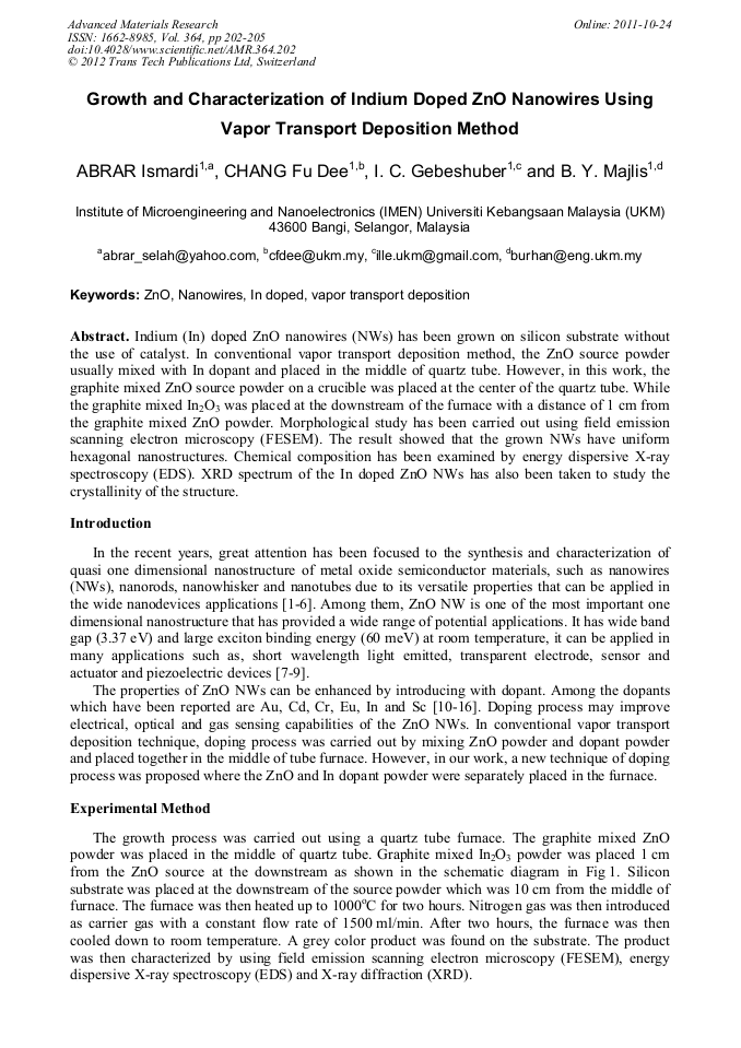
Indium (In) doped ZnO nanowires (NWs) has been grown on silicon substrate without the use of catalyst. In conventional vapor transport deposition method, the ZnO source powder usually mixed with In dopant and placed in the middle of quartz tube. However, in this work, the graphite mixed ZnO source powder on a crucible was placed at the center of the quartz tube. While the graphite mixed In2O3 was placed at the downstream of the furnace with a distance of 1 cm from the graphite mixed ZnO powder. Morphological study has been carried out using field emission scanning electron microscopy (FESEM). The result showed that the grown NWs have uniform hexagonal nanostructures. Chemical composition has been examined by energy dispersive X-ray spectroscopy (EDS). XRD spectrum of the In doped ZnO NWs has also been taken to study the crystallinity of the structure.

You might also be interested in these eBooks

Info:

Periodical:

Pages:

202-205

Citation:

Online since:

October 2011

Export:

Price:

Permissions CCC:

Permissions PLS:

Сopyright:

© 2012 Trans Tech Publications Ltd. All Rights Reserved

Share:

Citation:

[1] J. H. Shin, J. Y. Song and H. M. Park, Materials Letters, 2009. 63(1): pp.145-147.

Google Scholar

[2] F. Fang, D. X. Zhao, J. Y. Zhang , D. Z. Shen, Y. M. Lu, X. W. Fan, B. H. Li and X. H. Wang, Materials Letters, 2008. 62(6-7): pp.1092-1095.

Google Scholar

[3] H. Y. Ning, S. S. Guang, C. Wuyuan, Li. Xin, Z.C. Chun and H. Xun, Microelectronics Journal, 2009. 40(3): pp.517-519.

DOI: 10.1016/j.mejo.2008.06.082

Google Scholar

[4] A. Umar, S. H. Kim, J. H. Kim, and Y. B. Hahn, Materials Letters, 2008. 62(1): pp.167-171.

Google Scholar

[5] C. F. Dee, B. Y. Majlis, M. Yahaya and M. M. Salleh, Sains Malaysiana, 2008. 37(3): pp.281-283.

Google Scholar

[6] Y. C. Chin, M. Yahaya, M. M. Salleh and C. F. Dee, Sains Malaysiana, 2008. 37(3): pp.277-280.

Google Scholar

[7] M. H. Huang, Y. Wu, H. Feick, N. Tran, E. Weber, and P. Yang, Advanced Materials, 2001. 13(2): pp.113-116.

Google Scholar

[8] N. V. Hieu and N. D. Chien, Physica B: Condensed Matter, 2008. 403(1): pp.50-56.

Google Scholar

[9] J. Zhang, M. K. Li, L. Y. Yu, L. L. Liu, H. Zhang and Z. Yang, Applied Physics A: Materials Science & Processing, 2009. 97(4): pp.869-876.

Google Scholar

[10] N. Hongsith, C. Viriyaworasakul, P. Mangkorntong, N. Mangkorntong and S. Choopun, Ceramics International, 2008. 34(4): pp.823-826.

DOI: 10.1016/j.ceramint.2007.09.099

Google Scholar

[11] J. Z. Liu, P. X. Yan, G. H. Yue, J. B. Chang, R. F. Zhuo and D. M. Qu, Materials Letters, 2006. 60(25-26): pp.3122-3125.

DOI: 10.1016/j.matlet.2006.02.056

Google Scholar

[12] D. Chua, Y. P. Zeng and D. Jianga, Solid State Communications, 2007. 143(6-7): pp.308-312.

Google Scholar

[13] P. Mohanty, B. Kim. and J. Park, Materials Science and Engineering, 2007. 138(2007): p.4.

Google Scholar

[14] J. Jie, G. Wang, X. Han, Q. Yu, Y. Liao, G. Li and J.G. Hou , Chemical Physics Letters, 2004. 387(4-6): pp.466-470.

DOI: 10.1016/j.cplett.2004.02.045

Google Scholar

[15] J. Zhao, X. Yan, Y. Yang, Y. Huang and Y. Zhang, Materials Letters, 2010. 64(5): pp.569-572.

Google Scholar

[16] S.M. Zhou, X.H. Zhang, X.M. Meng, X. Fan, S. K. Wu and S.T. Lee, Physica E: Low-dimensional Systems and Nanostructures, 2005. 25(4): pp.587-591.

DOI: 10.1016/j.physe.2004.09.016

Google Scholar