Finite Element Analysis on Structural Stress of 8×8 Infrared Focal Plane Array Integrating with Microlens Arrays

Article Preview

Abstract:

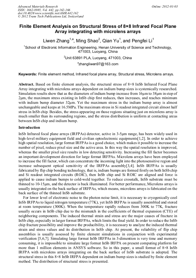
Based on finite element analysis, the structural stress of 8×8 InSb Infrared Focal Plane Array integrating with microlens arrays dependent on indium bump sizes is systemically researched. Simulation results show that as the diameters of indium bump increase from 16μm to 38μm in step of 2μm, the maximum stress existing in InSb chip first reduces, then increases, and reaches minimum with indium bump diameter 32μm. Yet the maximum stress in the indium bump array is almost unchangeable and keeps at 16.5MPa. The maximum stress in Si readout integrated circuit almost half stress in InSb chip. Besides, the stress appearing on those regions situating just on microlens array is much smaller than its surrounding regions, and the stress distribution is uniform at contacting areas between InSb chip and indium bump.

You might also be interested in these eBooks

Info:

Periodical:

Pages:

162-166

Citation:

Online since:

January 2012

Export:

Price:

Permissions CCC:

Permissions PLS:

Сopyright:

© 2012 Trans Tech Publications Ltd. All Rights Reserved

Share:

Citation:

[1] Y. Gau, L. Dai, S. Yang, and S. Yang, et al., Proceedings of SPIE, vol. 4078 (2003), p.467.

Google Scholar

[2] W. Parrish, J. Blackwell, G. Kincaid, and R. Paulson, Proceedings of SPIE, vol. 1540 (1991), p.274.

Google Scholar

[3] A. Tuantranont, V. M. Bright, J. Zhang, et al., Sensors and Actuators A, vol. 91 (2001), p.363.

Google Scholar

[4] Sihai Chen, Xinjian Yi, Hongchen Wang, et al., International Journal of Infrared and Millimeter Waves, Vol. 23 (2002), p.705.

Google Scholar

[5] Q.D. Meng, J.X. Li, Y. Q Lv, et al., Open Electrical&Electronic Engineering J., vol. 5 (2011), p.19.

Google Scholar

[6] Z. Zhang and C.P. Wong. IEEE Trans. Adv. Packaging, vol. 27 (2004), p.515.

Google Scholar

[7] L.W. Zhang, J.C. Wang, Q. Yu, et al., Advanced Materials Research, vol. 314-316 (2011), p.530.

Google Scholar

[8] S. Kim and H. Ledbetter: Materials Science and Engineering A, Vol. 252 (1998), p.139.

Google Scholar

[9] E.B. Hermida, D.G. Melo, J.C. Aguiar, et al., J. Alloys and Compounds, Vol. 310 (2000), p.91.

Google Scholar

[10] R. W. Chang and F. Patrick Mccluskey, J. Electronic Materials, Vol. 38 (2009), p.1855.

Google Scholar

[11] Chen. L, Zhang. Q, Wang. G, et al., Chinese J. Semiconductors, Vol. 22 (2001), p.107.

Google Scholar