p.187
p.193
p.199
p.206
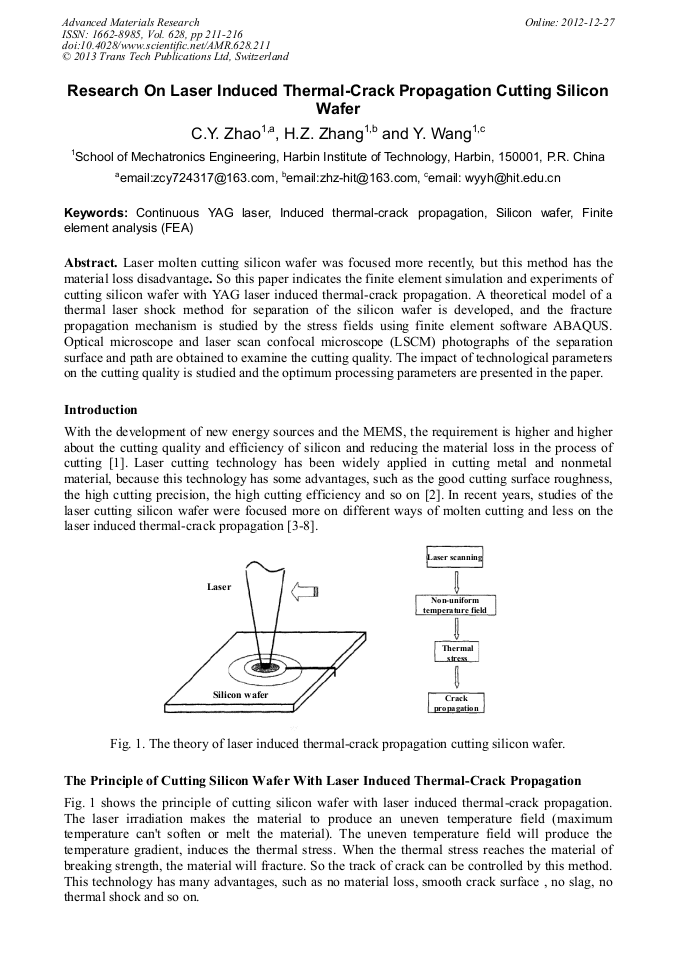
p.211
p.217
p.223
p.229
p.240
Research on Laser Induced Thermal-Crack Propagation Cutting Silicon Wafer

Abstract:
Laser molten cutting silicon wafer was focused more recently, but this method has the material loss disadvantage. So this paper indicates the finite element simulation and experiments of cutting silicon wafer with YAG laser induced thermal-crack propagation. A theoretical model of a thermal laser shock method for separation of the silicon wafer is developed, and the fracture propagation mechanism is studied by the stress fields using finite element software ABAQUS. Optical microscope and laser scan confocal microscope (LSCM) photographs of the separation surface and path are obtained to examine the cutting quality. The impact of technological parameters on the cutting quality is studied and the optimum processing parameters are presented in the paper.
Info:
Periodical:
Pages:
211-216
DOI:
Citation:
Online since:
December 2012
Authors:
Price:
Сopyright:
© 2013 Trans Tech Publications Ltd. All Rights Reserved
Share:
Citation: