Study on the Automobile Exhaust Thermoelectric Generator Test Bench
p.514
p.514
The Mechanism for the Production of Coherent Structures near Wall of a Turbulent Boundary Layer Excited by Wall Local Impulse Disturbance
p.521
p.521
The Thermo-Mechanical Coupling Analysis of Disc Brakes Transient Temperature Field
p.525
p.525
Nano Mechanical Behaviors of Hindleg Cuticle in Beetle Dorcus titanus (Coleoptera: Lucanidae)
p.529
p.529
Numerical Simulation of Laser Soldering about Electronic Connectors
p.534
p.534
Influence of Preheated Wire on GMAW Process
p.538
p.538
Structure Evolving at Bonding Interface of Dual-Alloys Jointed with Different Method under Coupling Action of Heat and Force
p.543
p.543
Preparation of Several Ionic Liquids with Excellent Friction-Reducing and Antiwear Properties
p.547
p.547
Thermal Stratification Effects on Surge Line Fatigue Life Based on Finite Element Analysis
p.551
p.551
Numerical Simulation of Laser Soldering about Electronic Connectors

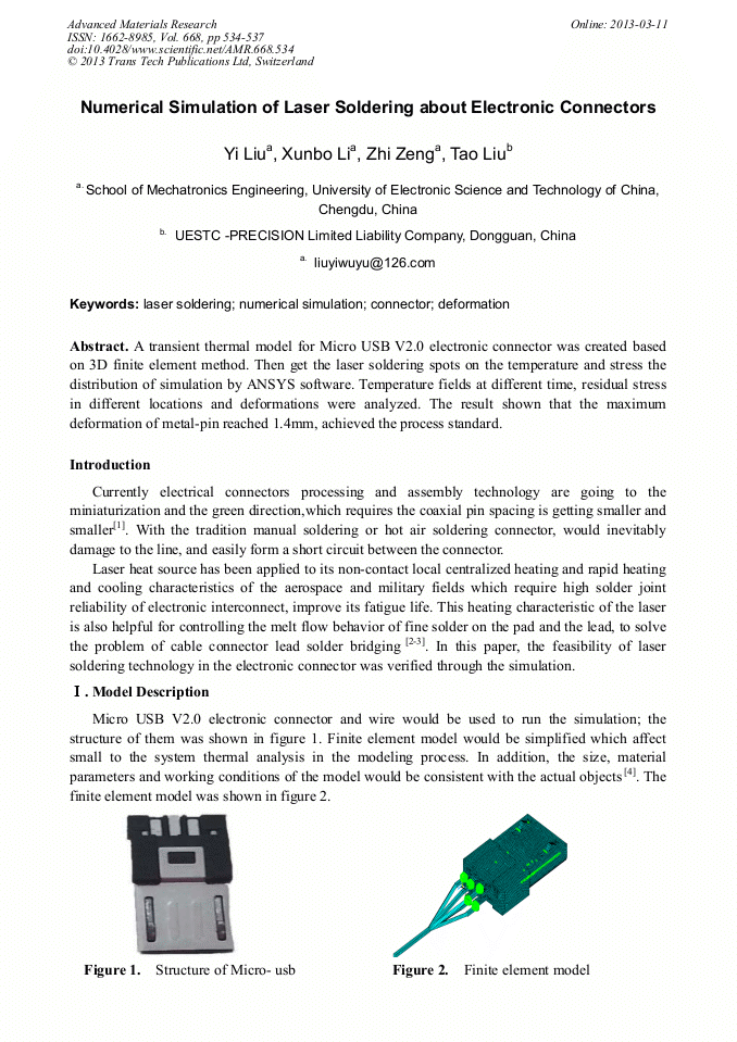
Abstract:
A transient thermal model for Micro USB V2.0 electronic connector was created based on 3D finite element method. Then get the laser soldering spots on the temperature and stress the distribution of simulation by ANSYS software. Temperature fields at different time, residual stress in different locations and deformations were analyzed. The result shown that the maximum deformation of metal-pin reached 1.4mm, achieved the process standard.
You might also be interested in these eBooks

Info:
Periodical:
Advanced Materials Research (Volume 668)
Pages:
534-537
DOI:
Citation:
Online since:
March 2013
Keywords:
Price:
Сopyright:
© 2013 Trans Tech Publications Ltd. All Rights Reserved
Share:
Citation: