Lateral Non-Uniformity Charges Influence on Interface Trap Density (Dit) by Terman Method in the nMOS Fabrication

Article Preview

Abstract:

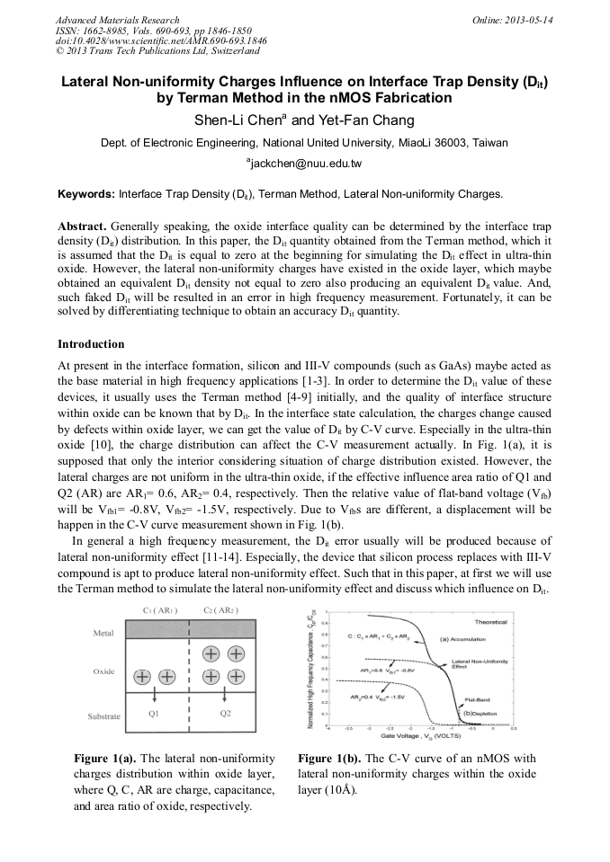
Generally speaking, the oxide interface quality can be determined by the interface trap density (Dit) distribution. In this paper, the Dit quantity obtained from the Terman method, which it is assumed that the Dit is equal to zero at the beginning for simulating the Dit effect in ultra-thin oxide. However, the lateral non-uniformity charges have existed in the oxide layer, which maybe obtained an equivalent Dit density not equal to zero also producing an equivalent Dit value. And, such faked Dit will be resulted in an error in high frequency measurement. Fortunately, it can be solved by differentiating technique to obtain an accuracy Dit quantity.

You might also be interested in these eBooks

Info:

Periodical:

Advanced Materials Research (Volumes 690-693)

Pages:

1846-1850

Citation:

Online since:

May 2013

Export:

Price:

Permissions CCC:

Permissions PLS:

Сopyright:

© 2013 Trans Tech Publications Ltd. All Rights Reserved

Share:

Citation:

[1] T.S. Lay, M. Hong, J. Kwo, J.Kwo, J. P. Mannaerts, W. H. Hung, D.J Huang: Solid State Electronics, Vol.1679 (2001), p.145.

DOI: 10.1016/s0038-1101(01)00175-7

Google Scholar

[2] A. Shirane, M. Otsuru, Sang-Yeop Lee, S. Yonezawa, S. Tanoi, H. Ito, N. Ishihara, K. Masu: IEEE Radio Frequency Integrated Circuits Symposium (RFIC 2012), p.455.

DOI: 10.1109/rfic.2012.6242320

Google Scholar

[3] S. Salleh, M.F. Hashim, A.A.A. Rahman, Z.A. Majid: IEEE Symposium on Wireless Technology and Applications (ISWTA 2012), p.56.

Google Scholar

[4] L. M. Terman: Solid-State Electronics, Vol.284 (1962), p.5.

Google Scholar

[5] E.H. Nicollian, J.R. Brews: MOS Physics and Technology (Wiley, New Jersey, 1982), Chap.8, p.328.

Google Scholar

[6] A. Koukab, A. Bath and E. Losson: Solid-State Electronics, Vol.635 (1997), p.41.

Google Scholar

[7] D. K. Schroder: Semiconductor Material and Device Characterization (Wiley, New York, 1998) 2nd ed., Chap.6, p.377.

Google Scholar

[8] Hao-Peng Lin and Jenn-Gwo Hwu: IEEE Transactions on Electron Devices, Vol.54, Issue 11 (2007), p.3064.

Google Scholar

[9] David A. Deen, James G. Champlain: Applied Physics Letters, Vol.99, Issue 5 (2011), p.53501.

Google Scholar

[10] James B. Kuo: International Workshop on Electron Devices and Semiconductor Technology, (EDST 2007), p.37.

Google Scholar

[11] J. G. Hwu and W. S. Wang: Applied Physics A, Vol.41 (1986), p.40.

Google Scholar

[12] S. Berberich, P. Godignon, M. L. Locatelli, J. Millan and H. L. Hartnagel: Solid-State Electronics, Vol.915 (1998), p.42.

DOI: 10.1016/s0038-1101(98)00122-1

Google Scholar

[13] P. Ozdag, E. Atanassova, M.Gunes: Journal of Optoelectronics and Advanced Materials, Vol.293 (2005), p.7.

Google Scholar

[14] I. Starkov, A. Starkov, S. Tyaginov, H. Enichlmair, H. Ceric, T. Grasser: International Semiconductor Device Research Symposium (ISDRS 2011), p.1.

DOI: 10.1109/isdrs.2011.6135359

Google Scholar