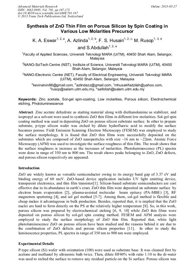
Synthesis of ZnO Thin Film on Porous Silicon by Spin Coating in Various Low Molarities Precursor

Article Preview

Abstract:

Zinc acetate dehydrate as starting material along with diethanolamine as stabilizer, and isopropyl as a solvent were used to synthesis ZnO thin films in different low molarities. Sol-gel spin coating method was used in depositing ZnO on porous silicon substrate surface. In other to prepare substrate, p-type silicon wafer was etched by dilute hydrofluoric acid to modify the surface becomes porous. Field Emission Scanning Electron Microscopy (FESEM) was employed to study the surface morphology. It is found that ZnO thin films were successfully deposited on the substrates which are composed of ZnO nanoparticles with size ~16 nm to ~22nm. Atomic Force Microscopy (AFM) was used to investigate the surface roughness of thin film. The result shows that the surface roughness is increase as the increases of molarities. Photoluminescence (PL) spectra were done in range of 350 nm to 800 nm. The result shows peaks belonging to ZnO, ZnO defects, and porous silicon respectively are appeared.

You might also be interested in these eBooks

Info:

Periodical:

Pages:

167-171

Citation:

Online since:

May 2013

Export:

Price:

Permissions CCC:

Permissions PLS:

Сopyright:

© 2013 Trans Tech Publications Ltd. All Rights Reserved

Share:

Citation:

[1] Y. Zhang, W. Fa, F. Yang, Z. Zheng and P. Zhang, Ionics 16 (9), 815-820 (2010).

Google Scholar

[2] M. G. Varnamkhasti, H. R. Fallah and M. Zadsar, Vacuum 86 (7), 871-875 (2012).

Google Scholar

[3] S. K. Min, G. Y. Kwang, L. Jae-Young, K. Soaram, N. Giwoong, L. Dong-Yul, S. K. Jin and S. K. Jong, Journal of the Korean Physical Society 59 (3), 2354 (2011).

Google Scholar

[4] F. Yang, S. Ma, X. Zhang, M. Zhang, F. Li, J. Liu and Q. Zhao, Superlattices and Microstructures 52 (2), 210-220 (2012).

Google Scholar

[5] M. Caglar, S. Ilican, Y. Caglar and F. Yakuphanoglu, Applied Surface Science 255 (8), 4491-4496 (2009).

DOI: 10.1016/j.apsusc.2008.11.055

Google Scholar

[6] R. G. Singh, F. Singh, V. Agarwal and R. M. Mehra, Journal of Physics D: Applied Physics 40 (10), 3090-3093 (2007).

Google Scholar

[7] Q.-l. Ma, B.-g. Zhai and Y. M. Huang, Journal of Sol-Gel Science and Technology (2012).

Google Scholar

[8] M. S. Kim, S. Kim, G. Nam, D.-Y. Lee and J.-Y. Leem, Optical Materials 34 (9), 1543-1548 (2012).

Google Scholar

[9] H. Cai, H. Shen, Y. Yin, L. Lu, J. Shen and Z. Tang, Journal of Physics and Chemistry of Solids 70 (6), 967-971 (2009).

Google Scholar

[10] H. C. Hsu, C. S. Cheng, C. C. Chang, S. Yang, C. S. Chang and W. F. Hsieh, Nanotechnology 16 (2), 297-301 (2005).

Google Scholar

[11] E. Kayahan, Journal of Luminescence 130 (7), 1295-1299 (2010).

Google Scholar

[12] G. Singh, S. B. Shrivastava, D. Jain, S. Pandya and V. Ganesan, Defect and Diffusion Forum 293, 99-105 (2009).

DOI: 10.4028/www.scientific.net/ddf.293.99

Google Scholar

[13] M. Wang, J. Wang, W. Chen, Y. Cui and L. Wang, Materials Chemistry and Physics 97 (2-3), 219-225 (2006).

Google Scholar

[14] M. Balucani, P. Nenzi, E. Chubenko, A. Klyshko and V. Bondarenko, Journal of Nanoparticle Research 13 (11), 5985-5997 (2011).

DOI: 10.1007/s11051-011-0346-7

Google Scholar

[15] X. L. Huang, S. Y. Ma, L. G. Ma, H. Q. Bian and C. Su, Physica E: Low-dimensional Systems and Nanostructures 44 (1), 190-195 (2011).

DOI: 10.1016/j.physe.2011.08.013

Google Scholar

[16] S. K. Min, G. Y. Kwang, L. Jae-Young, K. Soaram, N. Giwoong, Y. K. Do, K. Sung-O, L. Dong-Yul, S. K. Jin and S. K. Jong, Journal of the Korean Physical Society 59 (2), 346 (2011).

Google Scholar

[17] M. S. Kim, K. G. Yim, D. Y. Kim, S. Kim, G. Nam, D.-Y. Lee, S.-O. Kim, J. S. Kim, J. S. Kim, J.-S. Son and J.-Y. Leem, Electronic Materials Letters 8 (1), 75-80 (2012).

DOI: 10.1007/s13391-011-0130-y

Google Scholar