Structural and Optical Properties of α-Ga2O3 Films Deposited on Sapphire (10‾10) and (01‾12) Substrate by MOCVD

Article Preview

Abstract:

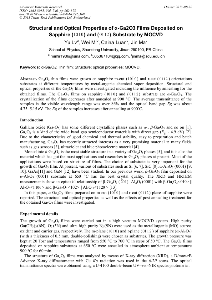
Ga2O3 thin films were grown on sapphire m-cut () and r-cut () orientations substrates at different temperatures by metal-organic chemical vapor deposition. Structural and optical properties of the Ga2O3 films were investigated including the influence by annealing for the obtained films. The Ga2O3 films on sapphire () and () substrate are α-Ga2O3. The crystallization of the films decreases after annealed at 900 °C. The average transmittance of the samples in the visible wavelength range was over 86% and the optical band gap Eg was about 4.755.15 eV. The Eg of the samples increases after annealing at 900 °C.

You might also be interested in these eBooks

Info:

Periodical:

Pages:

369-373

Citation:

Online since:

August 2013

Export:

Price:

Permissions CCC:

Permissions PLS:

Сopyright:

© 2013 Trans Tech Publications Ltd. All Rights Reserved

Share:

Citation:

[1] A.F. Pasquevich, M. Uhrmacher, L. Ziegeler, K.P. Lieb, Phys. Rev. B 48 (1993) 10053-62.

Google Scholar

[2] O. Takayoshi, A. Naoki, S. Norihito, O. Shigeo, F. Shizuo, Thin Solid Films 516 (2008) 5768-5771.

Google Scholar

[3] T. Schwebel, M. Fleischer, H. Meixner, C. -D. Kohl, Sensors and Actuators B 49 (1998) 46-51.

Google Scholar

[4] S. Nakamura, Science, 281 (1998) 956-961.

Google Scholar

[5] Y. Zhang, J. Yan, Q. Li, C. Qu, L. g Zhang, et al. , Materials Science and Engineering B 176 (2011) 846–849.

Google Scholar

[6] M. Passlack, E. F. Schubert, W. S. Hobson, M. Hong, N. Moriya et al., J. Appl. Phys. 77, (1995) 686-693.

Google Scholar

[7] A. Trinchi, S. Kaciulis, L. Pandolfi, M.K. Ghantasala, Y.X. Li et al., Sensor Actuat. B 103 (2004) 129–135.

Google Scholar

[8] G. A. Battiston, R. Gerbasi, M. Porchia, R. Bertoncello, F. Caccavale,Thin Solid Films 279 (1996) 115-118.

DOI: 10.1016/0040-6090(95)08161-5

Google Scholar

[9] Y. Kokubun, K. Miura, F. Endo, S. Nakagomi, Appl. Phys. Lett 90 (2007) 031912.

Google Scholar

[10] M. Orit, H. Hiramatsu , H. Ohta , M. Hirano , H. Hosono, Thin Solid Films 411 (2002) 134–139.

Google Scholar

[11] Z. Yu, C. D. Overgaard, R. Droopad, M. Passlack, Appl. Phys. Lett. 82 (2003) 2978.

Google Scholar

[12] C. Lee, H. Chen, F. Hwang, H. Lee, J. Elec. Mater. 34 (2005) 282-286.

Google Scholar

[13] Y. Lv, J. Ma, W. Mi, C. Luan, Z. Zhu, H. Xiao, Vacuum 86 (2012) 1850-1854.

Google Scholar

[14] G. Mills, Z. G. Li, D. Meisel, J. Phys. Chem. 92 (1988) 822.

Google Scholar