Electrical Properties of Nanostructured Titanium Dioxide Thin Films Prepared by Sol-Gel Spin-Coating Method

Article Preview

Abstract:

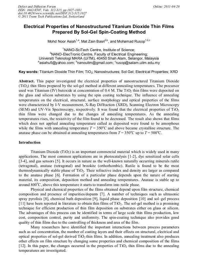
This paper investigated the electrical properties of nanostructured Titanium Dioxide (TiO2) thin films prepared by the sol-gel method at different annealing temperatures. The precursor used was Titanium (IV) butoxide at concentration of 0.4 M. The TiO2 thin films were deposited on the glass and silicon substrates by using the spin coating technique. The influence of annealing temperatures on the electrical, structural, surface morphology and optical properties of the films were characterized by I-V measurement, X-Ray Diffraction (XRD), Scanning Electron Microscopy (SEM) and UV-Vis Spectroscopy, respectively. It was found that the electrical properties of TiO2¬ thin films were changed due to the changes of annealing temperatures. As the annealing temperatures rises, the resistivity of the film found to be decreased. The result also shows that films which does not applied annealing temperature called as deposited were found to be amorphous while the films with annealing temperature T = 350oC and above became crystalline structure. The anatase phase can be obtained at annealing temperatures from T = 350oC up to T = 500oC.

You might also be interested in these eBooks

Info:

Periodical:

Defect and Diffusion Forum (Volumes 312-315)

Pages:

1027-1031

Citation:

Online since:

April 2011

Export:

Price:

Permissions CCC:

Permissions PLS:

Сopyright:

© 2011 Trans Tech Publications Ltd. All Rights Reserved

Share:

Citation:

[1] K.L. Yeung, S.T. Yau, A.J. Maira, J.M. Coronado et al.: J. Catalysis Vol. 219 (2003), p.107.

Google Scholar

[2] J.M. Arabatzis, T. Stergiopoulos, D. Andreeva, S. Kitova, S.G. Neophytides, and P. Falaras: J. Catalysis Vol. 220 (2003), p.127.

Google Scholar

[3] J.H. Yoon, S.R. Jang, R. Vittal, J. Lee, and K.J. Kim: Journal of Photochemistry and Photobiology A: Chemistry Vol. 180 (2006), p.184.

Google Scholar

[4] I.C. Flores, J.N.D. Freitas, C. Longo, M.A.D. Paoli, H. Winnischofer, A.F. Nogueira: Journal of Photochemistry and Photobiology A: Chemistry Vol. 189 (2007), p.153.

DOI: 10.1016/j.jphotochem.2007.01.023

Google Scholar

[5] M.R. Mohammadi, D.J. Fray, Cordero-Cabrera: Sensors and Actuators B Vol. 124 (2007), p.74.

Google Scholar

[6] H. Bach, D. Krause: Thin films on Glass, Springer, Heidelberg, (1997).

Google Scholar

[7] C.J. Brinker, G.W. Scherrer, Sol–Gel Science, Academic, San Diego, (1990).

Google Scholar

[8] M. Dj. Blesic, Z.V. Saponjic, J.M. Nedeljkovic, and D.P. Uskokovic: Materials Letters Vol. 54 (2002), p.298.

Google Scholar

[9] A.M. More, T.P. Gujar, J.L. Gunjakar et al.: Appl. Surf. Sci. Vol. 255 (2008), p.2682.

Google Scholar

[10] A.V. Valiulis and P. Silickas: Journal of Achievements in materials and manufacturing engineering Vol. 24 (2007), p.188.

Google Scholar

[11] A.I. Kontosa, A.G. Kontosa, D.S. Tsouklerisa, M.C. Bernardc, N. Spyrellis, and P. Falarasa: Journal of Materials Processing Technology Vol. 196 (2008), p.243.

Google Scholar

[12] M.K. Ahmad, N.A. Rasheid, A. Zain Ahmed, S. Abdullah, and M. Rusop: American Institute of Physics (AIP) Vol. 1017 (2007), p.109.

Google Scholar