Characterization of Diamond Spherical Shell Thick Film by DC Plasma CVD

Article Preview

Abstract:

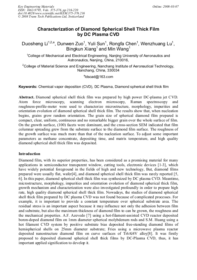
Diamond spherical shell thick film was prepared by high power DC-plasma jet CVD. Atom force microscopy, scanning electron microscopy, Raman spectroscopy and roughness-profile-meter were used to characterize microstructure, morphology, impurities and orientation evolution of diamond spherical shell thick film. The results show that, when nucleation begins, grains grow random orientation. The grain size of spherical diamond film prepared is compact, clear, uniform, continuous and no remarkable bigger grain over the whole surface of film. On the growth surface, (100) facets were dominant, and the cross-section SEM indicated that film columnar spreading grew from the substrate surface to the diamond film surface. The roughness of the growth surface was much more than that of the nucleation surface. To adjust some important parameters as methane concentrate, depositing time, and matrix temperature, and high quality diamond spherical shell thick film was deposited.

You might also be interested in these eBooks

Info:

Periodical:

Key Engineering Materials (Volumes 375-376)

Pages:

216-220

Citation:

Online since:

March 2008

Export:

Price:

Permissions CCC:

Permissions PLS:

Сopyright:

© 2008 Trans Tech Publications Ltd. All Rights Reserved

Share:

Citation:

[1] H.W. Chen and V. Rudolph: Diamond and Related Materials, Vol. 12 (2003), p.1633.

Google Scholar

[2] S.M. Huang, Franklin and C.N. Hong: Surface & Coating Technology, Vol. 200 (2006), p.3153.

Google Scholar

[3] R. Ikeda, M. Hayashi and A. Yonezu: Diamond and Related Materials, Vol. 13 (2004), pp. (2024).

Google Scholar

[4] D.W. Zuo, S.L. Song and B. K Xiang: Key Engineering Materials, Vols. 258-259 (2004), p.517.

Google Scholar

[5] R.F. Chen, D.W. Zuo and D.S. Li: Key Engineering Materials, Vols. 315-316 (2006), p.742.

Google Scholar

[6] V.J. Tiroldi, E.J. Corat and A.F. Pena: Diamond and Related Materials, Vol. 4 (1995), p.1255.

Google Scholar

[7] A.F. Azevedo, R.C. Mendes de Barros and S.H.P. Serrano: Surface & Coating Technology, Vol. 200 (2006), p.5975.

Google Scholar

[8] M.D. Fries and Y.K. Vohra: J. Appl. Phys., Vol. 35 (2002), p.105.

Google Scholar

[9] D.S. Li, D.W. Zuo and R.F. Chen: Key Engineering Materials, Vol. 315-316 (2006), p.385.

Google Scholar

[10] C.J. Tang, A.J. Neves and A.J.S. Fernandes: Diamond and Related Materials, Vol. 12 (2003), p.1411.

Google Scholar

[11] D.W. Park and J.S. Yun: Thin Solid Film, Vol. 345 (1999), p.60.

Google Scholar

[12] B. Lunn, D.A. Wright and L.Y. Zhang: Diamond and Related Materials, Vol. 7 (1998), p.129.

Google Scholar

[13] S.H. Seo, T.H. Lee and J.S. Park: Diamond and Related Materials, Vol. 12 (2003), p.1670.

Google Scholar