Growth Temperature, Microstructural Differences and Light-Induced Changes in a-Si:H Deposited on Glass Substrates
p.147
p.147
Positron Beam Study of Defects Induced in Ar-Implanted Si
p.150
p.150
Positron Annihilation Study of Formation of Mg Vacancy in MgO
p.153
p.153
Search for Positron Trapping at Quantum-Dot Like Cu Nano Particles on the Surface of Fe Using Positron Annihilation induced Auger Electron Spectroscopy (PAES)
p.156
p.156
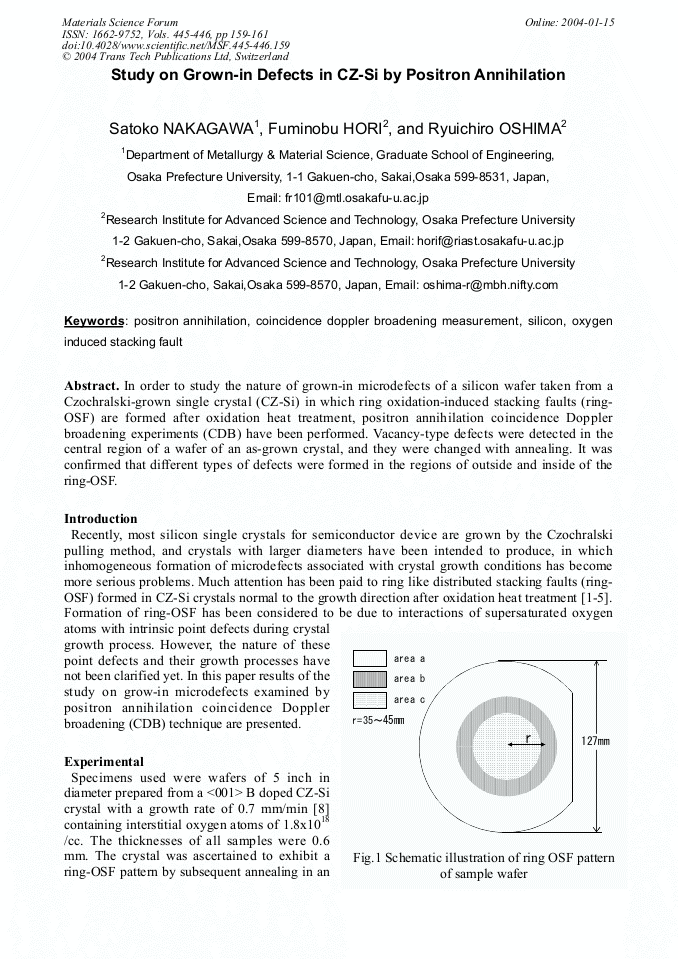
Study on Grown-in Defects in CZ-Si by Positron Annihilation
p.159
p.159
Identification of Positron Trapping Sites in Nanocrystalline ZnFe2O4 by Coincidence Doppler Broadening Measurements
p.162
p.162
Vacancy-Solute Binding Energies in Aluminum by Positron Annihilation
p.165
p.165
Irradiation-Enhanced Cu-Precipitation in Fe-Cu Alloys Studied by Positron Annihilation Spectroscopy and Electrical Resistivity Measurement
p.168
p.168
Vacancy-Like Defects in Doped Pb(Zr60Ti40)O3 Observed by Positron Lifetime and Coincident Doppler Spectroscopy
p.171
p.171
Study on Grown-in Defects in CZ-Si by Positron Annihilation

Abstract:
You might also be interested in these eBooks
Info:
Periodical:
Materials Science Forum (Volumes 445-446)
Pages:
159-161
Citation:
Online since:
January 2004
Authors:
Price:
Сopyright:
© 2004 Trans Tech Publications Ltd. All Rights Reserved
Share:
Citation: