Influence of Fabrication Parameter on the Nanostructure of SiNWs under HF/AgNO3/Fe(NO3)3 Etching System

Article Preview

Abstract:

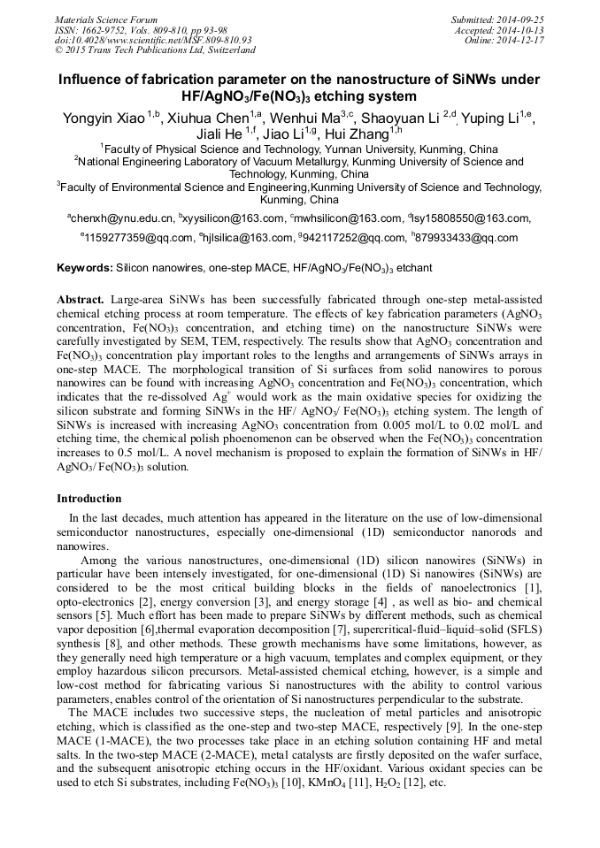
Large-area SiNWs has been successfully fabricated through one-step metal-assisted chemical etching process at room temperature. The effects of key fabrication parameters (AgNO3 concentration, Fe (NO3)3 concentration, and etching time) on the nanostructure SiNWs were carefully investigated by SEM, TEM, respectively. The results show that AgNO3 concentration and Fe (NO3)3 concentration play important roles to the lengths and arrangements of SiNWs arrays in one-step MACE. The morphological transition of Si surfaces from solid nanowires to porous nanowires can be found with increasing AgNO3 concentration and Fe (NO3)3 concentration, which indicates that the re-dissolved Ag+ would work as the main oxidative species for oxidizing the silicon substrate and forming SiNWs in the HF/ AgNO3/ Fe (NO3)3 etching system. The length of SiNWs is increased with increasing AgNO3 concentration from 0.005 mol/L to 0.02 mol/L and etching time, the chemical polish phoenomenon can be observed when the Fe (NO3)3 concentration increases to 0.5 mol/L. A novel mechanism is proposed to explain the formation of SiNWs in HF/ AgNO3/ Fe (NO3)3 solution.

You might also be interested in these eBooks

Info:

Periodical:

Materials Science Forum (Volumes 809-810)

Pages:

93-98

Citation:

Online since:

December 2014

Export:

Price:

Permissions CCC:

Permissions PLS:

Сopyright:

© 2015 Trans Tech Publications Ltd. All Rights Reserved

Share:

Citation:

* - Corresponding Author

[1] V. Schmidt, H. Riel,S. Senz, S. Karg, W. Riess, U. Gösele: Small, Vol. 41 (2002) No. 14, p.2590.

Google Scholar

[2] J. Goldberger, A. I. Hochbaum , R. Fan , P. Yang: Nano Letters, Vol. 286 (2005) No. 2, p.536.

Google Scholar

[3] B. Tian, X. Zheng, T. J. Kempa, Y. Fang: Nature, Vol. 50 (2011) No. 14, p.59.

Google Scholar

[4] K. Q. Peng , Y. Xu , Y. Wu, Y. J. Yan, S. T. Lee , J. Zhu: Small, Vol. 16 (2004) No. 9, p.1725.

Google Scholar

[5] E. C. Garnett, P. D. Yang, J. Am: Chemistry of Materials, Vol. 50 (2011) No. 26, p.5947.

Google Scholar

[6] Y. J. Hwang, A. Boukai , P. D. Yang: Nano Letters, Vol. 15 (20009) No. 47, p.3427.

Google Scholar

[7] C. K. Chan, H. L. Peng, G. Liu, K. McIlwrath, R. A. Huggins, Y. Cui, Nat: Nanotechnology, Vol. 40 (2008) No. 23, p.1289.

Google Scholar

[8] Y. Cui, Q. Wei, H. Park, C. M. Lieber: Science, Vol. 73 (2001) No. 41, p.1711.

Google Scholar

[9] F. Patolsky , G. Zheng , C. M. Lieber: Chemistry of Materials, Vol. 33 (2011) No. 23, p.2457.

Google Scholar

[10] J. Westwater, D. P. Gosain, S. Tomiya, S. Usui, H. Ruda: Journal of Colloid and Interface Science, Vol. 41 (2002) No. 14, p.2590.

Google Scholar

[11] N. Wang, Y. F. Zhang, Y. H. Tang, C. S. Lee, S. T. Lee: Integrated Ferroelectrics, Vol. 75(2008) No. 3, p. (1937).

Google Scholar

[12] Y. F. Zhang, Y. H. Tang, C. Lam, N. Wang, C. S. Lee, I. Bello: Advanced Functional Materials, Vol. 115(2008) No. 3, p.497.

Google Scholar

[13] J. D. Holmes, K. P. Johnston, R. C. Doty, B. A. Korgel: Science, Vol. 892 (2000) No. 1-2, p.47.

Google Scholar