p.505
p.511
p.517
p.521
p.528
p.533
p.543
p.550
p.555
Design of Digital Receiver Based on FPGA

Abstract:
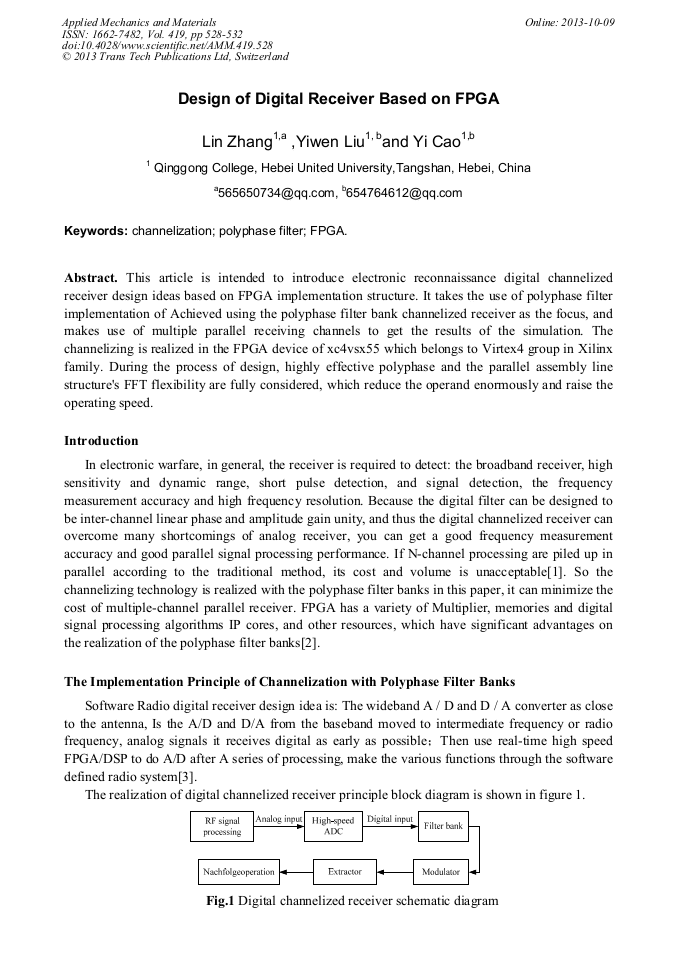
This article is intended to introduce electronic reconnaissance digital channelized receiver design ideas based on FPGA implementation structure. It takes the use of polyphase filter implementation of Achieved using the polyphase filter bank channelized receiver as the focus, and makes use of multiple parallel receiving channels to get the results of the simulation. The channelizing is realized in the FPGA device of xc4vsx55 which belongs to Virtex4 group in Xilinx family. During the process of design, highly effective polyphase and the parallel assembly line structure's FFT flexibility are fully considered, which reduce the operand enormously and raise the operating speed.
Info:
Periodical:
Pages:
528-532
DOI:
Citation:
Online since:
October 2013
Authors:
Keywords:
Price:
Сopyright:
© 2013 Trans Tech Publications Ltd. All Rights Reserved
Share:
Citation: