Design of Laptop Power Adapter Circuit

Article Preview

Abstract:

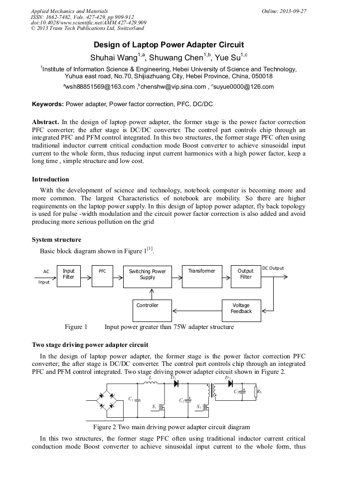
In the design of laptop power adapter, the former stage is the power factor correction PFC converter; the after stage is DC/DC converter. The control part controls chip through an integrated PFC and PFM control integrated. In this two structures, the former stage PFC often using traditional inductor current critical conduction mode Boost converter to achieve sinusoidal input current to the whole form, thus reducing input current harmonics with a high power factor, keep a long time , simple structure and low cost.

You might also be interested in these eBooks

Info:

Periodical:

Pages:

909-912

Citation:

Online since:

September 2013

Export:

Price:

Permissions CCC:

Permissions PLS:

Сopyright:

© 2013 Trans Tech Publications Ltd. All Rights Reserved

Share:

Citation:

[1] Xingjian Li Achievement of Fly back switching power quasi- resonant converter [J]. Electrical applications, 2005, 24(3), 110-111.

Google Scholar

[2] Ming Lumen Yang, Yelong Qiu Automatic Current technology and load sharing IC controllerUC3907 [J]. Electrical applications, 1999, 26(10), 27-30.

Google Scholar

[3] Y. Jang, M.M. Jovanovic, D.L. Dillman. Hold-up time extension circuit with integrated magnetizes[C]. IEEE APEC, 2005, 219-225.

DOI: 10.1109/apec.2005.1452923

Google Scholar

[4] Zhou X, Donati M, Amoroso L, ET al. Improved light-load efficiency for synchronous rectifier voltage regulator module. IEEE Transactions on Power Electronics, 2000, 15(5), 826-834.

DOI: 10.1109/63.867671

Google Scholar

[5] Wang T G, Zhou Xian Lee F C. A low voltage high efficiency and high power density DC/DC converter, IEEE Power Electronics Specialists Conference, record, (1997).

DOI: 10.1109/pesc.1997.616732

Google Scholar