Controlled Morphologies of Nanostructured ZnO Films by MOCVD Method

Article Preview

Abstract:

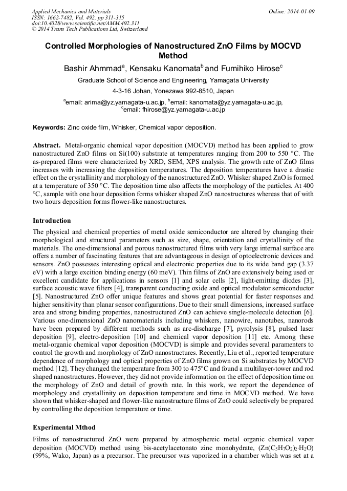
Metal-organic chemical vapor deposition (MOCVD) method has been applied to grow nanostructured ZnO films on Si (100) substrate at temperatures ranging from 200 to 550 °C. The as-prepared films were characterized by XRD, SEM, XPS analysis. The growth rate of ZnO films increases with increasing the deposition temperatures. The deposition temperatures have a drastic effect on the crystallinity and morphology of the nanostructured ZnO. Whisker shaped ZnO is formed at a temperature of 350 °C. The deposition time also affects the morphology of the particles. At 400 °C, sample with one hour deposition forms whisker shaped ZnO nanostructures whereas that of with two hours deposition forms flower-like nanostructures.

You might also be interested in these eBooks

Info:

Periodical:

Pages:

311-315

Citation:

Online since:

January 2014

Export:

Price:

Permissions CCC:

Permissions PLS:

Сopyright:

© 2014 Trans Tech Publications Ltd. All Rights Reserved

Share:

Citation:

[1] A. Wei, L. Pan, W. Huang : Mater. Sci. Eng., B, vol. 176 (2011), p.1409.

Google Scholar

[2] L. Lu, R. Li, K. Fan, T. Peng : Sol. Energy, vol. 84 (2010), p.844.

Google Scholar

[3] Q. Qiao, B.H. Li, C.X. Shan, J.S. Liu, J. Yu, X.H. Xie, Z.Z. Zhang, T.B. Ji, Y. Jia, D.Z. Shen: Mater. Lett., vol. 74 (2012), p.104.

Google Scholar

[4] N.W. Emanetoglu, C. Gorla, Y. Liu, S. Liang, Y. Lu : Mater. Sci. Semicond. Process., vol. 2 (1999), p.247.

Google Scholar

[5] Y. J. Chen, Y.Y. Shih, C.H. Ho, J.H. Du, Y.P. Fu : Ceram. Int., vol. 36(1) (2010), p.69.

Google Scholar

[6] S. K. Arya, S. Saha, J. E. Ramirez-Vick, V. Gupta, S. Bhansali, S. P. Singh : Anal. Chim. Acta, vol. 737 (2012), p.1.

Google Scholar

[7] A. A. Ashkarran, A. I. zada, S. M. Mahdavi, M. M. Ahadian : Mater. Chem. Phys., vol. 118 (2009), p.6.

Google Scholar

[8] C. Eberspacher, A. L Fahrenbruch, R. H Bube : Thin Solid Films, vol. 136 (1) (1986), p.1.

Google Scholar

[9] N.J. Ianno, L. McConville, N. Shaikh, S. Pittal, P.G. Snyder : Thin Solid Films, vol. 220 (1-2) (1992), p.92.

DOI: 10.1016/0040-6090(92)90554-o

Google Scholar

[10] R. Chander, A.K. Raychaudhuri : Solid State Comm., vol. 145 (2008), p.81.

Google Scholar

[11] F. Hirose, M. Ito, K. Kurita : Jpn J. Appl. Phys., vol. 47 (2008), p.5619.

Google Scholar

[12] C.Y. Liu, B.P. Zhang, N.T. Binh, K. Wakatsuki, Y. Segawa : J. Cryst. Growth, vol. 290 (2006), p.314.

Google Scholar

[13] J. -Y. Lee, D. Yin, S. Horiuchi : Chem. Mater., vol. 17 (2005), p.5498.

Google Scholar

[14] F. Jamal-Sheini : Ceram. Int., vol. 38 (2012), p.3649.

Google Scholar