p.133
p.139
p.145
p.149
p.155
p.161
p.166
p.170
p.179
A Design of Image Acquisition System Based on FPGA and USB2.0

Abstract:
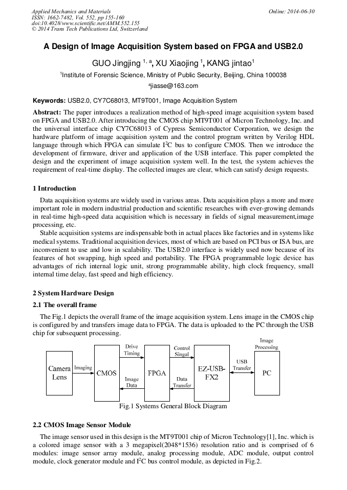
The paper introduces a realization method of high-speed image acquisition system based on FPGA and USB2.0. After introducing the CMOS chip MT9T001 of Micron Technology, Inc. and the universal interface chip CY7C68013 of Cypress Semiconductor Corporation, we design the hardware platform of image acquisition system and the control program written by Verilog HDL language through which FPGA can simulate I2C bus to configure CMOS. Then we introduce the development of firmware, driver and application of the USB interface. This paper completed the design and the experiment of image acquisition system well. In the test, the system achieves the requirement of real-time display. The collected images are clear, which can satisfy design requests.

Info:
Periodical:
Pages:
155-160
DOI:
Citation:
Online since:
June 2014
Authors:
Keywords:
Price:
Сopyright:
© 2014 Trans Tech Publications Ltd. All Rights Reserved
Share:
Citation: