p.818
p.822
p.826
p.830
p.836
p.840
p.844
p.848
p.852
Image Acquisition System Design of Camera Based on FPGA

Abstract:
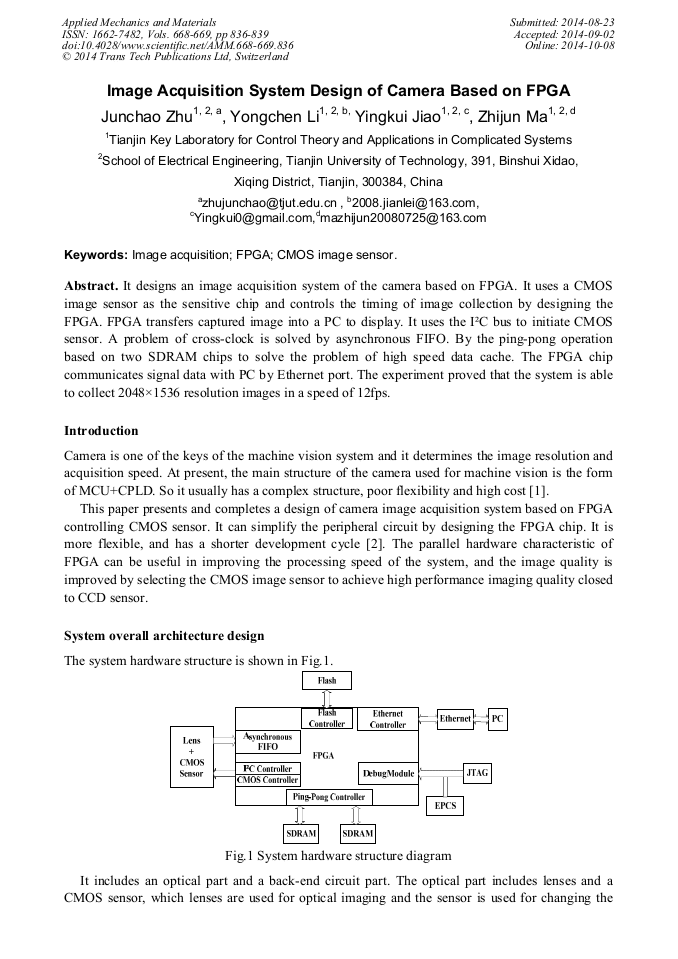
It designs an image acquisition system of the camera based on FPGA. It uses a CMOS image sensor as the sensitive chip and controls the timing of image collection by designing the FPGA. FPGA transfers captured image into a PC to display. It uses the I2C bus to initiate CMOS sensor. A problem of cross-clock is solved by asynchronous FIFO. By the ping-pong operation based on two SDRAM chips to solve the problem of high speed data cache. The FPGA chip communicates signal data with PC by Ethernet port. The experiment proved that the system is able to collect 2048×1536 resolution images in a speed of 12fps.

Info:
Periodical:
Pages:
836-839
Citation:
Online since:
October 2014
Authors:
Keywords:
Price:
Сopyright:
© 2014 Trans Tech Publications Ltd. All Rights Reserved
Share:
Citation: