Simulation and Analysis of DDR3 Bus Based on Fly-By Topology with Cadence

Article Preview

Abstract:

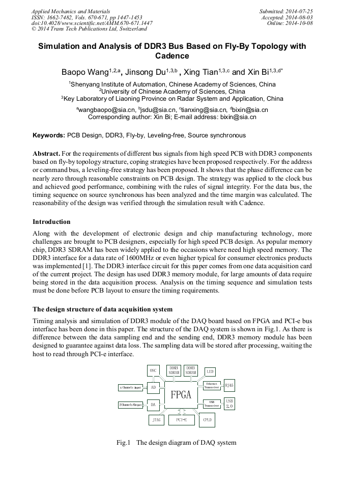
For the requirements of different bus signals from high speed PCB with DDR3 components based on fly-by topology structure, coping strategies have been proposed respectively. For the address or command bus, a leveling-free strategy has been proposed. It shows that the phase difference can be nearly zero through reasonable constraints on PCB design. The strategy was applied to the clock bus and achieved good performance, combining with the rules of signal integrity. For the data bus, the timing sequence on source synchronous has been analyzed and the time margin was calculated. The reasonability of the design was verified through the simulation result with Cadence.

You might also be interested in these eBooks

Info:

Periodical:

Pages:

1447-1453

Citation:

Online since:

October 2014

Export:

Price:

Permissions CCC:

Permissions PLS:

Сopyright:

© 2014 Trans Tech Publications Ltd. All Rights Reserved

Share:

Citation:

* - Corresponding Author

[1] F. June, S. Ralf, H. Lan, Y. Lu: Signal and power integrity for a 1600 Mbps DDR3 PHY in wirebond package. Electronic Components and Technology Conference. v1(2005), pp.284-290.

Google Scholar

[2] C. Brennan, C. Tudor, E. Schroeter, H. Wunschmann and S. Bokhari: Signal Integrity and PCB layout considerations for DDR2-800 Mb/s and DDR3 Memories. CDNLIVE Silicon Valley, Cadence(2007).

Google Scholar

[3] JESD79-3E. JEDEC DDR3 SDRAM Specification. 2010. 07.

Google Scholar

[4] M. Phil, A.H. Feras: Challenges in implementing DDR3 memory interface on PCB systems: A methodology for interfacing DDR3 SDRAM DIMM to an FPGA. International Engineering Consortium, Design Con(2008), pp.545-556.

Google Scholar

[5] Z. Fan, Z. Han: Research and design of timing on source synchronous clock system based on Hyperlynx. 2013 IEEE Conference Anthology, ANTHOLOGY (2013).

DOI: 10.1109/anthology.2013.6784987

Google Scholar

[6] J. Li, J. Hu, Y. Cao, L. Shi, L. Xiao. Computer Science (in Chinese). 2012, 39(4), pp.293-295.

Google Scholar

[7] M. Catrambone: Design Implementation of DDR2/DDR3 Interfaces From a PCB Designer Perspective in Cadence Allegro. RTP IPC Designers Council, March Chapter Meeting. 2013. 03.

Google Scholar

[8] Information on http: /www. altera. com. Guidelines for Designing High-Speed FPGA PCBs.

Google Scholar

[9] L. Zhao, Q. Chen: Signal integrity analysis of high-speed differential Vias. Applied Mechanics and Materials, 2014, v548-549, pp.754-759.

DOI: 10.4028/www.scientific.net/amm.548-549.754

Google Scholar

[10] Information on http: /www. edadoc. com.

Google Scholar

[11] Information on http: /www. altera. com. Cyclone V Device Handbook.

Google Scholar

[12] W. Tang, C. Fan. Modern Electronic Technique (in Chinese). 2014, 37(8). pp.75-78.

Google Scholar