p.925
p.930
p.934
p.938
p.942
p.946
p.950
p.954
p.958
Design of a 10 Bit 2GHz Digital to Analog Converter Circuit

Abstract:
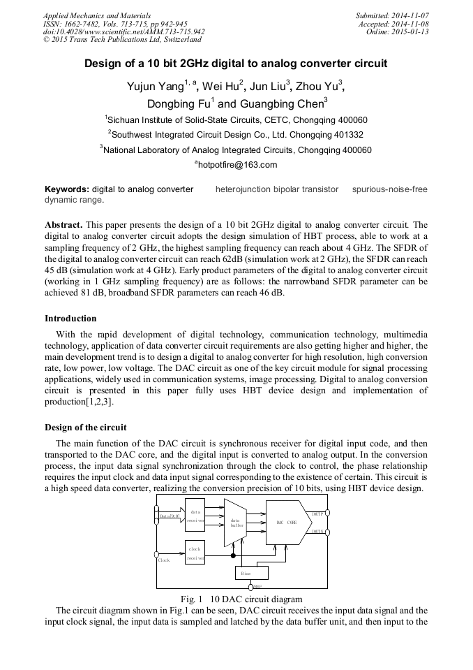
This paper presents the design of a 10 bit 2GHz digital to analog converter circuit. The digital to analog converter circuit adopts the design simulation of HBT process, able to work at a sampling frequency of 2 GHz, the highest sampling frequency can reach about 4 GHz. The SFDR of the digital to analog converter circuit can reach 62dB (simulation work at 2 GHz), the SFDR can reach 45 dB (simulation work at 4 GHz). Early product parameters of the digital to analog converter circuit (working in 1 GHz sampling frequency) are as follows: the narrowband SFDR parameter can be achieved 81 dB, broadband SFDR parameters can reach 46 dB.

Info:
Periodical:
Pages:
942-945
Citation:
Online since:
January 2015
Authors:
Price:
Сopyright:
© 2015 Trans Tech Publications Ltd. All Rights Reserved
Share:
Citation: