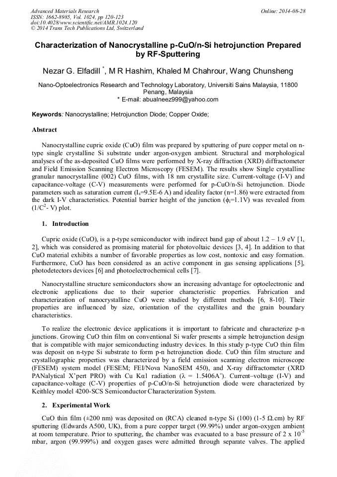
Characterization of Nanocrystalline p-CuO/n-Si Hetrojunction Prepared by RF-Sputtering

Article Preview

Abstract:

Normal 0 false false false EN-US X-NONE AR-SA /* Style Definitions */ table.MsoNormalTable {mso-style-name:"Table Normal"; mso-tstyle-rowband-size:0; mso-tstyle-colband-size:0; mso-style-noshow:yes; mso-style-priority:99; mso-style-parent:""; mso-padding-alt:0in 5.4pt 0in 5.4pt; mso-para-margin:0in; mso-para-margin-bottom:.0001pt; mso-pagination:widow-orphan; font-size:10.0pt; font-family:"Calibri","sans-serif";}Nanocrystalline cupric oxide (CuO) film was prepared by sputtering of pure copper metal on n-type single crystalline Si substrate under argon-oxygen ambient. Structural and morphological analyses of the as-deposited CuO films were performed by X-ray diffraction (XRD) diffractometer and Field Emission Scanning Electron Microscopy (FESEM). The results show Single crystalline granular nanocrystalline (002) CuO films, with 18 nm crystallite size. Current-voltage (I-V) and capacitance-voltage (C-V) measurements were performed for p-CuO/n-Si hetrojunction. Diode parameters such as saturation current (Is=9.5E-6 A) and ideality factor (n=1.86) were extracted from the dark I-V characteristics. Potential barrier height of the junction (ϕi=1.1V) was revealed from (1/C2- V) plot. Normal 0 false false false EN-US X-NONE AR-SA /* Style Definitions */ table.MsoNormalTable {mso-style-name:"Table Normal"; mso-tstyle-rowband-size:0; mso-tstyle-colband-size:0; mso-style-noshow:yes; mso-style-priority:99; mso-style-parent:""; mso-padding-alt:0in 5.4pt 0in 5.4pt; mso-para-margin:0in; mso-para-margin-bottom:.0001pt; mso-pagination:widow-orphan; font-size:10.0pt; font-family:"Calibri","sans-serif";}

You might also be interested in these eBooks

Info:

Periodical:

Pages:

120-123

Citation:

Online since:

August 2014

Export:

Price:

Permissions CCC:

Permissions PLS:

Сopyright:

© 2014 Trans Tech Publications Ltd. All Rights Reserved

Share:

Citation:

* - Corresponding Author

[1] T. Dimopoulos, A. Peić, P. Müllner, M. Neuschitzer, R. Resel, S. Abermann, M. Postl, E. List, S. Yakunin, W. Heiss. Journal of Renewable and Sustainable Energy, 5 (2013) 011205.

DOI: 10.1063/1.4791779

Google Scholar

[2] J. -P. Kim, E.S. Pak, T.E. Hong, J. -S. Bae, M.G. Ha, J.S. Jin, E.D. Jeong, K. Hong. JOURNAL OF CERAMIC PROCESSING RESEARCH, 13 (2012) S96-S99.

Google Scholar

[3] C. Wadia, A.P. Alivisatos, D.M. Kammen. Environmental Science & Technology, 43 (2009) 2072-(2077).

Google Scholar

[4] F. Alharbi, J.D. Bass, A. Salhi, A. Alyamani, H. -C. Kim, R.D. Miller. Renewable Energy, 36 (2011) 2753-2758.

DOI: 10.1016/j.renene.2011.03.010

Google Scholar

[5] C. Wang, L. Yin, L. Zhang, D. Xiang, R. Gao. Sensors, 10 (2010) 2088-2106.

Google Scholar

[6] S. Wang, C. Hsiao, S. Chang, K. Lam, K. Wen, S. Hung, S. Young, B. Huang. Sensors and Actuators A: Physical, 171 (2011) 207-211.

DOI: 10.1016/j.sna.2011.09.011

Google Scholar

[7] D. Chauhan, V. Satsangi, S. Dass, R. Shrivastav. Bulletin of Materials Science, 29 (2006) 709.

Google Scholar

[8] V. Palkar, P. Ayyub, S. Chattopadhyay, M. Multani. Physical Review B, 53 (1996) 2167.

Google Scholar

[9] Z. -s. Hong, Y. Cao, J. -f. Deng. Materials letters, 52 (2002) 34-38.

Google Scholar

[10] K. Borgohain, S. Mahamuni. Journal of materials research, 17 (2002) 1220-1223.

Google Scholar

[11] E. Darezereshki, F. Bakhtiari. Journal of Mining and Metallurgy, Section B: Metallurgy, 47 (2011) 73-78.

Google Scholar

[12] V. Quemener, L. Vines, E. Monakhov, B. Svensson. Thin solid films, 519 (2011) 5763-5766.

DOI: 10.1016/j.tsf.2010.12.204

Google Scholar

[13] T. Serin, S. Gürakar, N. Serin, N. Yıldırım, F.Ö. Kuş. Journal of Physics D: Applied Physics, 42 (2009) 225108.

DOI: 10.1088/0022-3727/42/22/225108

Google Scholar

[14] R.A. Ismail. Journal of Semiconductor Technology and Science, 9 (2009) 51.

Google Scholar