p.4683
p.4688
p.4693
p.4697
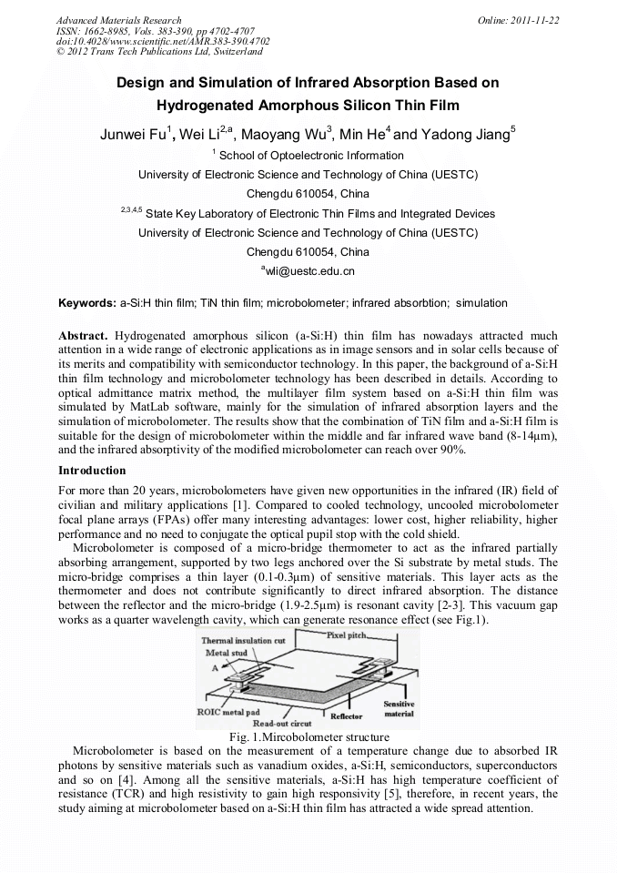
p.4702
p.4708
p.4715
p.4721
p.4727
Design and Simulation of Infrared Absorption Based on Hydrogenated Amorphous Silicon Thin Film

Abstract:
Hydrogenated amorphous silicon (a-Si:H) thin film has nowadays attracted much attention in a wide range of electronic applications as in image sensors and in solar cells because of its merits and compatibility with semiconductor technology. In this paper, the background of a-Si:H thin film technology and microbolometer technology has been described in details. According to optical admittance matrix method, the multilayer film system based on a-Si:H thin film was simulated by MatLab software, mainly for the simulation of infrared absorption layers and the simulation of microbolometer. The results show that the combination of TiN film and a-Si:H film is suitable for the design of microbolometer within the middle and far infrared wave band (8-14µm), and the infrared absorptivity of the modified microbolometer can reach over 90%.
Info:
Periodical:
Pages:
4702-4707
Citation:
Online since:
November 2011
Authors:
Keywords:
Price:
Сopyright:
© 2012 Trans Tech Publications Ltd. All Rights Reserved
Share:
Citation: