p.2225
p.2229
p.2234
p.2238
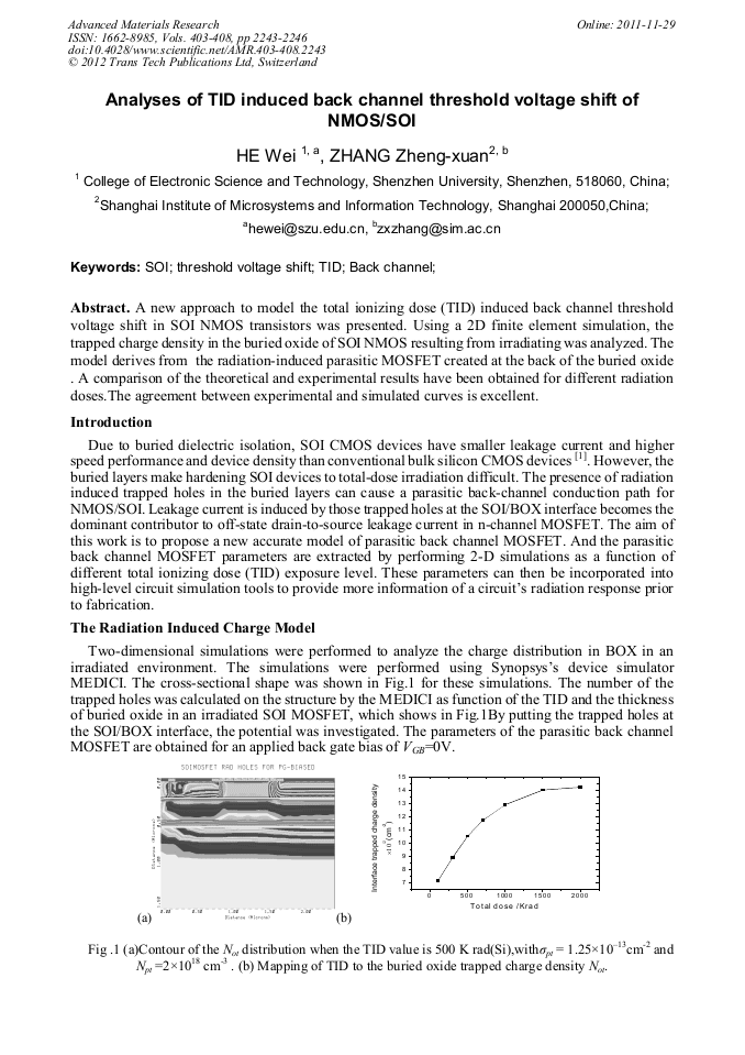
p.2243
p.2247
p.2251
p.2255
p.2259
Analyses of TID Induced Back Channel Threshold Voltage Shift of NMOS/SOI

Abstract:
A new approach to model the total ionizing dose (TID) induced back channel threshold voltage shift in SOI NMOS transistors was presented. Using a 2D finite element simulation, the trapped charge density in the buried oxide of SOI NMOS resulting from irradiating was analyzed. The model derives from the Radiation-Induced parasitic MOSFET created at the back of the buried oxide . A comparison of the theoretical and experimental results have been obtained for different radiation doses.The agreement between experimental and simulated curves is excellent.
Info:
Periodical:
Pages:
2243-2246
Citation:
Online since:
November 2011
Authors:
Keywords:
Price:
Сopyright:
© 2012 Trans Tech Publications Ltd. All Rights Reserved
Share:
Citation: