p.1781
p.1785
p.1790
p.1794
p.1798
p.1802
p.1806
p.1811
p.1815
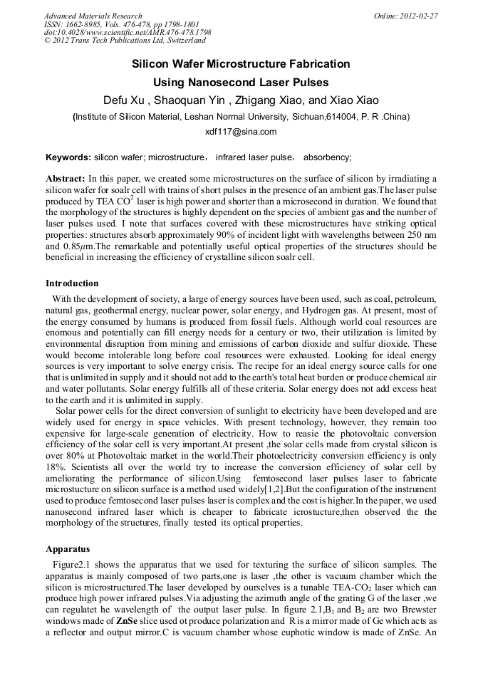
Silicon Wafer Microstructure Fabrication Using Nanosecond Laser Pulses
Abstract:
In this paper, we created some microstructures on the surface of silicon by irradiating a silicon wafer for soalr cell with trains of short pulses in the presence of an ambient gas.The laser pulse produced by TEA CO2 laser is high power and shorter than a microsecond in duration. We found that the morphology of the structures is highly dependent on the species of ambient gas and the number of laser pulses used. I note that surfaces covered with these microstructures have striking optical properties: structures absorb approximately 90% of incident light with wavelengths between 250 nm and 0.85μm.The remarkable and potentially useful optical properties of the structures should be beneficial in increasing the efficiency of crystalline silicon soalr cell.
Info:
Periodical:
Pages:
1798-1801
Citation:
Online since:
February 2012
Authors:
Keywords:
Price:
Сopyright:
© 2012 Trans Tech Publications Ltd. All Rights Reserved
Share:
Citation:


