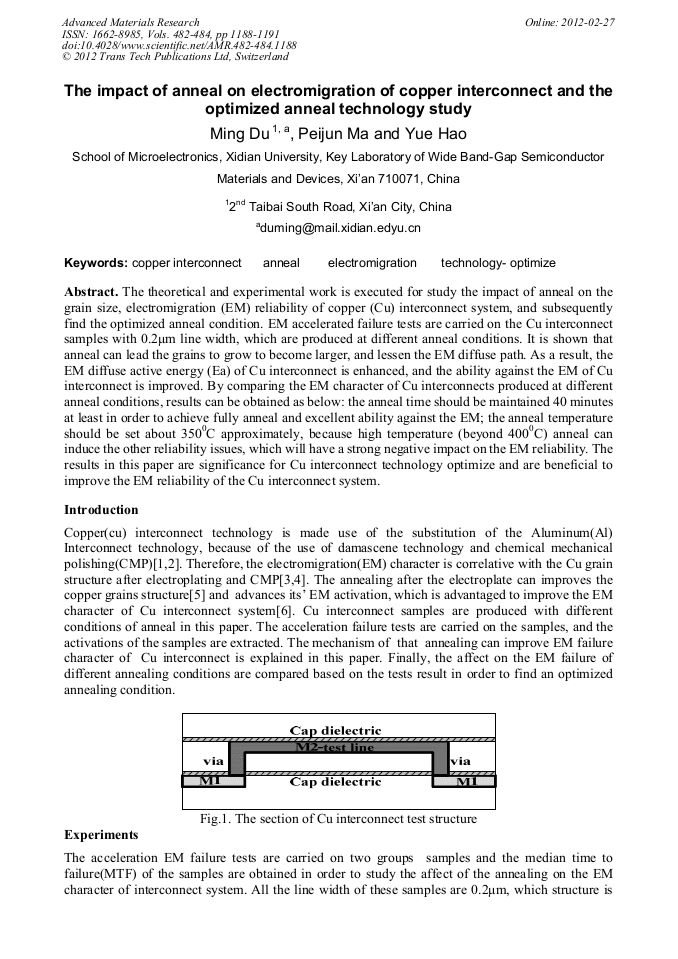
[8]
studies the phenomenon with the simulation of the growth of grains in the interconnection. The simulation result shown the grains size become lager when the annealing time become longer. (a)The MTF distribution with no annealing (b) The MTF distribution with annealing Fig.3. The tests result of the samples with or without annealing Anneal conditions No annealing 3500C,45min annealing EM activation Ea(eV) 0.91 1.02 Table 3. The activations of samples with or without annealing The mechanism is analyzed in physics based on the experiments and other researchers in this paper. It is thought that the interconnect lines can be treated as a system, which maintained a minimum energy state. Cu interconnect line is poly-crystal material. The grains grow up when the grains are heated, which can lead the mean grains size become larger. This phenomenon can decrease the system energy, which is related with grains boundary (GB). Because the existence of the instauration bonds and distortion bonds at the site of the grains boundary, the energy of the GB is higher than the energy inside the grains. So the reduction of the number of the GB can lead to the reduction of the energy of the interconnect system. Annealing can enlarge the grains size reduce the number of GB and reduce the system energy. As the result of the reduction of the number of GB, which is an important EM diffusion path, the EM diffusion is restrained. Therefore the diffusion activation of the Cu interconnect is improved, and the lifetime of the Cu interconnect is prolong. It is summarized that annealing can enlarge the grains size and increase the EM activation. It is an effective method to improve the EM character of the Cu interconnects system. But the improvement of the EM character is different with the different annealing conditions. The different anneal conditions are carried on six groups of samples, and the EM acceleration failure tests are implemented on the samples in order to find an optimized anneal conditions. The anneal conditions and tests result are shown in Table 4 and Fig.5. Anneal time samples Anneal temperatures 1st group 2nd group 3rd group g 4th group 5th group 6th group 1750C 1750C 3000C 3500C 3500C 4000C 15min 30min 30min 30min 45min 45min Table 4. Anneal conditions of interconnect samples Fig.5. The MTF distribution of the samples with different annealing The tests results of the optimized anneal condition are shown in Fig.5. It is shown that the EM lifetime of the interconnect increases apparently with the increase of the anneal time and temperature. But the improvement of the EM character is unconspicuous when the anneal temperature is higher than 4000C. It is revealed the effect of extends the anneal time is better than that of enhances the anneal temperature. That is, the EM character of the Cu interconnect can be improved markedly by a long time (>40min) annealing. Therefore, the anneal temperature should not exceed 4000C in order to obtained the excellent anneal effect. Conclusions The technology conditions have an important affection on the reliability of the Cu interconnect system. The annealing technology after electroplating can enlarge the Cu grains size, increase the EM activation, improve the reliability of the interconnect and prolong the lifetime. In addition, the improvement is different with the anneal conditions. According to the experiments and research in this paper, it is shown the anneal time should be beyond 40min, and the anneal temperature should maintained at about 3500C. If the anneal temperature is beyond 4000C, the other reliability issues can be occur. The results obtained in this paper are helpful to improve the reliability of the Cu interconnect, and have practical value for the production of the Cu interconnect system and the optimized technology condition. Referneces
Google Scholar
[1]
Alam T, Dhiman R, Chandel R, Solanki D 2011 International Conference on Emerging Trends in Electrical and Computer Technology, Hamirpur, India, March 23-24, 2011 p.697
DOI: 10.1109/icetect.2011.5760207
Google Scholar
[2]
Du M, Ma P J, Li S Y, Hao Y, Liu H X 2009 IEEE International Conference on Electron Devices and Solid-State Circuits, Shaanxi Xi'an, Dec 25-27 2009 p.14.
Google Scholar
[3]
Wu Z Y, Yang Y T, Chai C C, Li Y J, Wang J Y, Liu B 2008 Acta Phys. Vol.57 No.6 3730
Google Scholar
[4]
Gambino J P 2011 International Symposium on VLSI Technology Systems and Applications, Vermont USA, April 25-27 2011 p.1
Google Scholar
[5]
Zhang J M, Xu K W 2003 Acta Phys. Vol.52 No.1 145
Google Scholar
[6]
Alers G B, Domisch D 2001 IEEE 39th Annual International Reliability Physics Symposium, Orlando, Florida, Apr 30 2001 p.350
Google Scholar
[7]
Ogawa E T, Lee K D, Matsuhashi H, Ko K S, Justison P R, Ramamurthi A N, Bierwag A J, Ho P S, Blaschke V A, Havemann R H 2001 IEEE 39th Annual International Reliability Physics Symposium, Orlando, Florida, Apr 30 2001 p.341
DOI: 10.1109/relphy.2001.922925
Google Scholar
[8]
Walton D T, Frost H J, Thompson C V 1992 Appl. Phys. Lett. 61 40
Google Scholar