Feasibility to Fabricate the 45° Slant with Anisotropic Silicon Etching in NaOH Solution

Article Preview

Abstract:

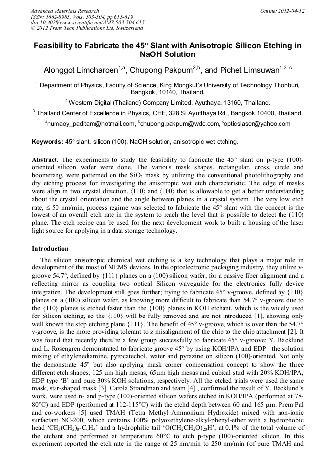
The experiments to study the feasibility to fabricate the 45 slant on p-type (100)-oriented silicon wafer were done. The various mask shapes, rectangular, cross, circle and boomerang, were patterned on the SiO2 mask by utilizing the conventional photolithography and dry etching process for investigating the anisotropic wet etch characteristic. The edge of masks were align in two crystal direction, 110 and 100 that is allowable to get a better understanding about the crystal orientation and the angle between planes in a crystal system. The very low etch rate,  50 nm/min, process regime was selected to fabricate the 45 slant with the concept is the lowest of an overall etch rate in the system to reach the level that is possible to detect the (110) plane. The etch recipe can be used for the next development work to built a housing of the laser light source for applying in a data storage technology.

You might also be interested in these eBooks

Info:

Periodical:

Advanced Materials Research (Volumes 503-504)

Pages:

615-619

Citation:

Online since:

April 2012

Export:

Price:

Permissions CCC:

Permissions PLS:

Сopyright:

© 2012 Trans Tech Publications Ltd. All Rights Reserved

Share:

Citation:

[1] M.J. Madou: Fundamentals of Microfabrication: The Science of Miniaturization, 2nd ed. CRC PRESS (2002).

Google Scholar

[2] I. Shubin, J.E. Cunningham, X. Zheng, J. Simons, D. Feng, H. Liang, C.C. Kung, M. Asghari and A.V. Krishnamoorthy: Optical Proximity Communication, Proc. Of SPIE Vol. 7219 (2009).

DOI: 10.1117/12.813415

Google Scholar

[3] Y. Bäcklund and L. Rosengren: New shapes in (100) Si using KOH and EDP etches, J. Micromech. Microeng., vol. 2 (1992), pp.75-79.

DOI: 10.1088/0960-1317/2/2/002

Google Scholar

[4] C. Strandman, L. Rosengren, Håkan G.A. Elderstig, and Y. Bäcklund: Fabrication of 45° Mirrors Together with Well-Defined V-Grooves Using Wet Anisotropic Etching of Silicon, Journal of microelectromechanical systems, Vol. 4, No. 4, (1995).

DOI: 10.1109/84.475548

Google Scholar

[5] P. Pal, K. Sato, M.A. Gosalvez and M. Shikida: Novel Wet Anisotropic Etching Process for the Realization of New Shapes of Silicon MEMS Structures, IEEE 978-1-4244-1858-9/07/$25. 00 (2007), pp.499-504.

DOI: 10.1109/mhs.2007.4420906

Google Scholar

[6] O. Powell and H. B. Harrison: Anisotropic etching of {100} and {110} planes in (100) silicon, J. Micromech. Microeng. 11 (2001), pp.217-220.

DOI: 10.1088/0960-1317/11/3/309

Google Scholar

[7] T. Ohkubo, K. Tanaka, T. Hirota, K. Itao, K. Kato, S. Ichihara, M. Ohmi, H. Maeda, T. Niwa, Y. Mitsuoka and K. Nakajima: High speed sub-micron bit detection using tapered aperture mounted optical slider flying above a patterned metal medium, Microsystem Technologies 9 (2003).

DOI: 10.1007/s00542-002-0272-9

Google Scholar

[8] M.H. Kryder, E.C. Gage, T.W. Mcdaniel, W.A. Challener, R.E. Rottmayer, G. Ju, Y.T. Hsia and M.F. Erden: Heat Assisted Magnetic Recording, Proceeding of the IEEE, Vol. 96 (2008) No. 11, pp.1810-1835.

DOI: 10.1109/jproc.2008.2004315

Google Scholar

[9] Wet-Chemical Etching and Cleaning of Silicon : www. virginiasemi. com.

Google Scholar