p.937
p.941
p.945
p.951
p.955
p.960
p.964
p.968
p.972
Design of Data Acquisition and Storage System for Digital and Analog Signal Based on FPGA

Abstract:
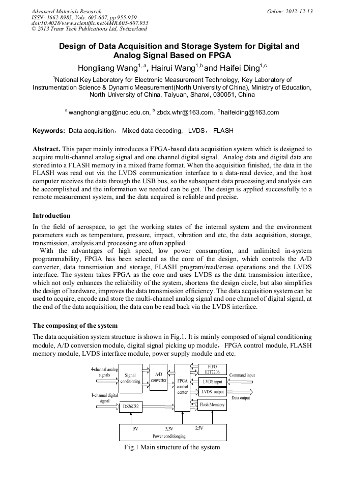
This paper mainly introduces a FPGA-based data acquisition system which is designed to acquire multi-channel analog signal and one channel digital signal. Analog data and digital data are stored into a FLASH memory in a mixed frame format. When the acquisition finished, the data in the FLASH was read out via the LVDS communication interface to a data-read device, and the host computer receives the data through the USB bus, so the subsequent data processing and analysis can be accomplished and the information we needed can be got. The design is applied successfully to a remote measurement system, and the data acquired is reliable and precise.
Info:
Periodical:
Pages:
955-959
Citation:
Online since:
December 2012
Authors:
Keywords:
Price:
Сopyright:
© 2013 Trans Tech Publications Ltd. All Rights Reserved
Share:
Citation: