p.884
p.887
p.892
p.896
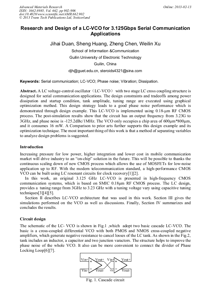
p.902
p.907
p.910
p.914
p.918
Research and Design of a LC-VCO for 3.125Gbps Serial Communication Applications

Abstract:
A LC voltage-control oscillator(LC-VCO) with two stage LC cross coupling structure is designed for serial communication applications. The design constraints and tradeoffs among power dissipation and startup condition, tank amplitude, tuning range are executed using graphical optimization method. This design strategy leads to a good phase noise performance which is demonstrated through design example. This LC-VCO is implemented using 0.18-m RF CMOS process. The post-simulation results show that the circuit has an output frequency from 3.23G to 3GHz, and phase noise is -125.2dBc/1MHz. The VCO only occupies a chip area of 600m*800m, and it consumes 16 mW. A Comparison to prior arts further supports this design example and its optimization technique. The most important thing of this work is that a method of separating variables to analyze design problems is suggested.

Info:
Periodical:
Pages:
902-906
DOI:
Citation:
Online since:
February 2013
Authors:
Keywords:
Price:
Сopyright:
© 2013 Trans Tech Publications Ltd. All Rights Reserved
Share:
Citation: