Diode Characteristics of Zinc Oxide Thin Film at Different Deposition Time for FET Applications

Article Preview

Abstract:

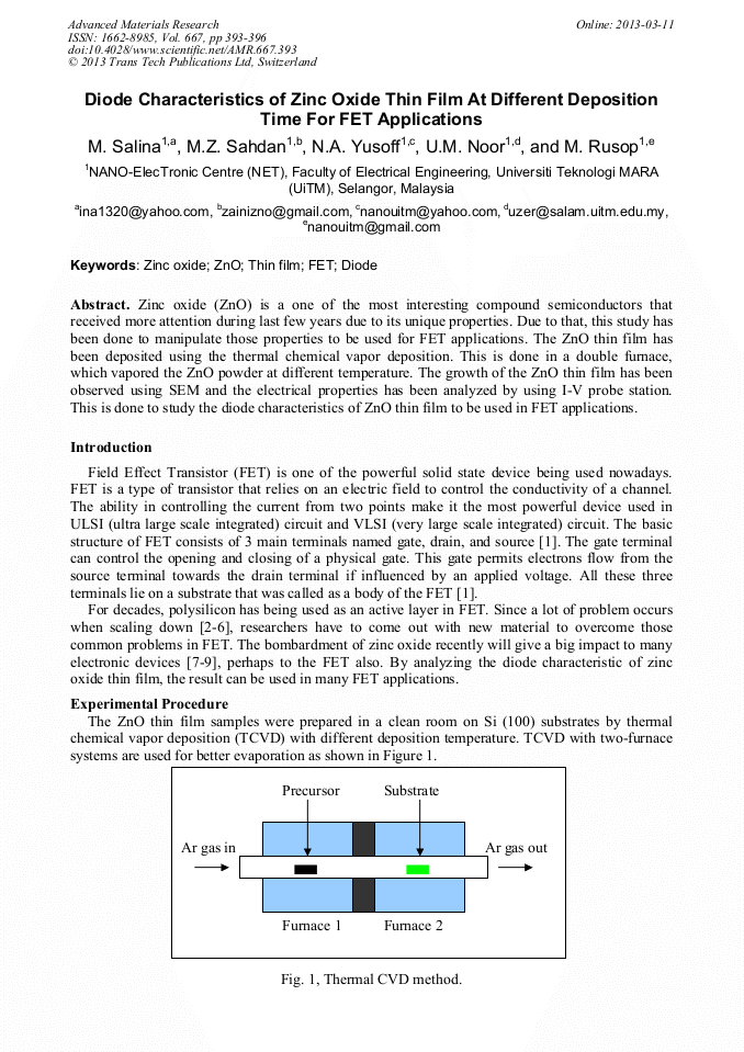
Zinc oxide (ZnO) is a one of the most interesting compound semiconductors that received more attention during last few years due to its unique properties. Due to that, this study has been done to manipulate those properties to be used for FET applications. The ZnO thin film has been deposited using the thermal chemical vapor deposition. This is done in a double furnace, which vapored the ZnO powder at different temperature. The growth of the ZnO thin film has been observed using SEM and the electrical properties has been analyzed by using I-V probe station. This is done to study the diode characteristics of ZnO thin film to be used in FET applications.

You might also be interested in these eBooks

Info:

Periodical:

Pages:

393-396

Citation:

Online since:

March 2013

Export:

Price:

Permissions CCC:

Permissions PLS:

Сopyright:

© 2013 Trans Tech Publications Ltd. All Rights Reserved

Share:

Citation:

[1] Richard C. Jaeger and Travis N. Blalock, Microelectronic Circuit Design, Mc Graw Hill International Edition, Chapter 4.

Google Scholar

[2] Robert Chau, Justin Brask, Suman Datta, and Gilbert Duwey, Application of High-k Gate Dielectrics and Metal Gate Electrodes to Enable Silicon and Non-silicon Logic Nanotechnology, Intel Corporation.

DOI: 10.1016/j.mee.2005.04.035

Google Scholar

[3] Scaling for High Performance CMOS: From SiO2 to High-k, Intel Corporation.

Google Scholar

[4] Intel Core Microarchitecture, Introducing the 45 nm Next Generation Intel Core Microarchitecture", Intel Corporation.

DOI: 10.1109/hotchips.2007.7482514

Google Scholar

[5] Jack C. Lee, H.J. Cho, C.S. Kuag, S. Rhee, and Y.H. Kim, High-k Dielectrics and MOSFET Characteristics, IEEE Electron Device Module (2003) 95-98.

Google Scholar

[6] Matthias Passlack, Ravi Droopad, and Karthik Rajagopalan, High Mobility NMOSFET Structure With High-k Dielectric, IEEE Electron Device Letter 26 (10) (2005) 713-715.

DOI: 10.1109/led.2005.856707

Google Scholar

[7] Vladimir A. Fonoberov and Alexander A. Balandin, Journal of Nanoelectronics and Optoelectronics 1 (2006) 19-38.

Google Scholar

[8] Oleg Lupan, Sergiu Shishiyanu, Lee Chow, Teodor Shishiyanu, Thin Solid Films 516 (2008) 3338-3345.

DOI: 10.1016/j.tsf.2007.10.104

Google Scholar

[9] Haoyong Yin, Zhude Xu, Qingsheng Wang, Jingyi Bai, Huahui Bao, Materials Chemistry and Physics 91 (2005) 130-133.

Google Scholar

[10] Zhao Guo Liang, Lin Bi Xia, Hong Liang, Meng Xiang Dong, and Fu Zhu Xi, Structural and Luminescent Properties of ZnO Thin Films Deposited by Atmospheric Pressure Chemical Vapour Deposition, ZHOA Guo-Liang et al., Chin. Phys. Lett. Vol. 21, No. 7 (2004).

DOI: 10.1088/0256-307x/21/7/055

Google Scholar

[11] L.L. Chen, H.P. He, Z.Z. Ye, Y.J. Zeng, J.G. Lu, B.H. Zhao, L.P. Zhu, Influence of post-annealing temperature on properties of ZnO: Li thin films, Chemical Physics Letters 420 (2006) 358-361.

DOI: 10.1016/j.cplett.2005.12.071

Google Scholar