The Study on Subsurface Damage Depth and Morphology of Optical Material

Article Preview

Abstract:

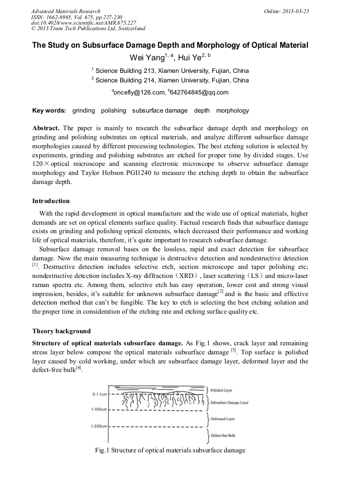
The paper is mainly to research the subsurface damage depth and morphology on grinding and polishing substrates on optical materials, and analyze different subsurface damage morphologies caused by different processing technologies. The best etching solution is selected by experiments, grinding and polishing substrates are etched for proper time by divided stages. Use 120×optical microscope and scanning electronic microscope to observe subsurface damage morphology and Taylor Hobson PGI1240 to measure the etching depth to obtain the subsurface damage depth.

You might also be interested in these eBooks

Info:

Periodical:

Pages:

227-230

Citation:

Online since:

March 2013

Authors:

Export:

Price:

Permissions CCC:

Permissions PLS:

Сopyright:

© 2013 Trans Tech Publications Ltd. All Rights Reserved

Share:

Citation:

[1] Yinxia Zhang. Detection on ultraprecise process suface/subsurface damage of monocrystalline silicon. IC engineer unicircuit and component, 2004, 7: 72~75.

Google Scholar

[2] Gailin Li, Yulie Wu, Zhuo Wang etc. Destructive detection technology on optical elements subsurface damage depth. Aviation precision manufacturing technology, 2006, 42(6): 19~22.

Google Scholar

[3] Shen J., Liu S.H., Yi K., et al. Subsurface damage in optical substrates. Optical, 2005, 116:288~294.

Google Scholar

[4] NingChen, Qinghua Zhang, Qiao Xu etc. Subsurface damage detection and chemical corrosion technology for K9. Strong laser and particles bunch, 2005, 17(9): 1289~1293.

Google Scholar

[5] Bi Zhang, JianMeng. Nanotechnology and precision engineering. Optical, 2003, 1(1):48~56.

Google Scholar

[6] Gailing Li, Kaiyuan Sun, Renyu Feng etc. Subsurface damage mechanism and detection method. Colliery machinery, 2008, 29(12): 99~100.

Google Scholar