Photoelectrochemical Behaviour of Copper Indium Selenide Thin Films

Article Preview

Abstract:

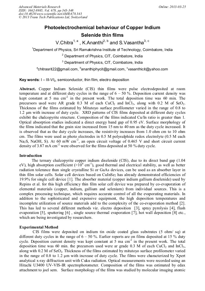
Copper Indium Selenide (CIS) thin films were pulse electrodeposited at room temperature and at different duty cycles in the range of 6 – 50 %. Deposition current density was kept constant at 5 ma cm-2 in the present work. The total deposition time was 60 min. The precursors used were AR grade 0.3 M of each CuCl2 and InCl3, along with 0.2 M of SeO2. Thickness of the films estimated by Mitutoyo surface profilometer varied in the range of 0.8 to 1.2 μm with increase of duty cycle. XRD patterns of CIS films deposited at different duty cycles exhibit the chalcopyrite structure. Composition of the films indicated Cu/In ratio is greater than 1. Optical absorption studies indicated a direct energy band gap of 0.95 eV. Surface morphology of the films indicated that the grain size increased from 15 nm to 40 nm as the duty cycle increased. It is observed that as the duty cycle increases, the resistvity increases from 1.0 ohm cm to 10 ohm cm. The films were used as photoelectrodes in 0.5 M polysulphide redox electrolyte (0.5 M each Na2S, NaOH, S). At 60 mW cm-2, an open circuit voltage of 0.465 V and short circuit current density of 3.87 mA cm-2 were observed for the films deposited at 50 % duty cycle.

You might also be interested in these eBooks

Info:

Periodical:

Pages:

343-348

Citation:

Online since:

March 2013

Export:

Price:

Permissions CCC:

Permissions PLS:

Сopyright:

© 2013 Trans Tech Publications Ltd. All Rights Reserved

Share:

Citation:

[1] Repins, I., Contreras, M.A., Egaas, B., DeHart, C., Scharf, J., Perkins, C.L., To, B., Noufi, R., Prog. Photovoltaics: Res. Appl. 16 (3), 235–239.

DOI: 10.1002/pip.822

Google Scholar

[2] Hermann, A.M., Gonzalez, C., Ramakrishnan, P.A., Balzar, D., Popa, N., Rice, P., Marshall, C.H., Hilfiker, J.N., Tiwald, T., Sebastian, P.J., Calixto, M.E., Bhattacharya, R.N., 2001 Solar energy mater. solar cells 70 (3), 345–361.

DOI: 10.1016/s0927-0248(01)00076-9

Google Scholar

[3] Lincot, D., Guillemoles, J.F., Taunier, S., Guimard, D., Sicx-Kurdi, J., Chaumont, A., Roussel, O., Ramdani, O., Hubert, C., Fauvarque, J.P., Bodereau, N., Parissi, L., Panheleux, P., Fanouillere, P., Naghavi, N., Grand, P.P., Benfarah, M., Mogensen, P., Kerrec, O., 2004. Solar Energy 77(6), 725–737.

DOI: 10.1016/j.solener.2004.05.024

Google Scholar

[4] Alaa, A.A., Afify, H.H., 2008. Mater. Res. Bull. 43 (6), 1539–1548.

Google Scholar

[5] Akl, A.A.S., Ashour, A., Ramadan, A.A., El-Hady, K.A., 2001. Vacuum 61, 75–84.

DOI: 10.1016/s0042-207x(00)00458-9

Google Scholar

[6] Muller, J., Nowoczin, J., Scmitt, H., 2006. Thin Solid Films 496, 364–370.

Google Scholar

[7] Klenk, M., Schenker, O., Alberts, V., Bucher, E., 2002. Semicond. Sci. Technol. 17, 435–439.

Google Scholar

[8] Agilan, S., Mangalaraj, D., Narayandass, Sa. K., Velumani, S., Ignatiev, A., 2007. Vacuum 81, 813–818.

DOI: 10.1016/j.vacuum.2006.08.002

Google Scholar

[9] D. Briggs, M.P. Seah, Practical Surface Analysis, Auger and X-ray Photoelectron Spectroscopy, second ed., vol. 1, John Wiley & Sons, New York, 1993.

Google Scholar

[10] A. Rochefort, J.C. Bertolini, M. Abon, P. Delichere, European workshop on refractory metals and silicides, Appl. Surf. Sci. 294 (1993) 43–52.

Google Scholar

[11] C.D. Wagner, W.M. Riggs, L.E. Davis, J.F. Moulder, in: G.E. Mullenberg (Ed.),Handbook of X-ray Photoelectron Spectroscopy, Minnesota, 1978.

Google Scholar

[12] J.H. Scho ¨n, V. Alberts, E. Bucher, Sharp optical emissions from Cu-rich, polycrystalline CuInSe2 thin films, J. Appl. Phys. 81 (6) (1997)2799–2802.

DOI: 10.1063/1.364306

Google Scholar