The Effect of Ternary Material (Zr, Y, and O) High-k Gate Dielectrics

Article Preview

Abstract:

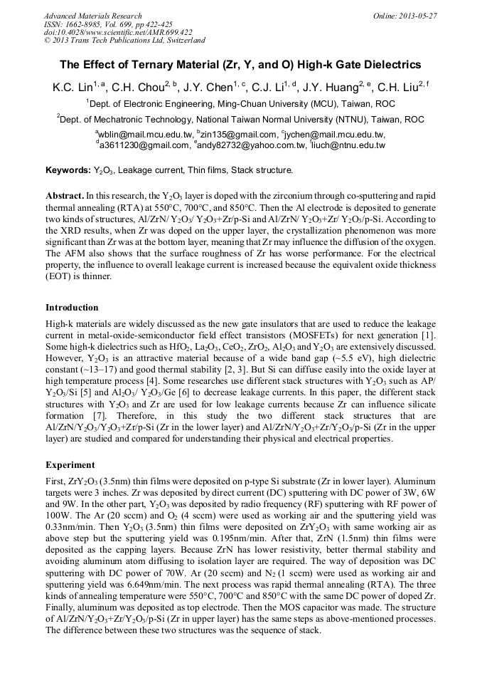
In this research, the Y2O3 layer is doped with the zirconium through co-sputtering and rapid thermal annealing (RTA) at 550°C, 700°C, and 850°C. Then the Al electrode is deposited to generate two kinds of structures, Al/ZrN/ Y2O3/ Y2O3+Zr/p-Si and Al/ZrN/ Y2O3+Zr/ Y2O3/p-Si. According to the XRD results, when Zr was doped on the upper layer, the crystallization phenomenon was more significant than Zr was at the bottom layer, meaning that Zr may influence the diffusion of the oxygen. The AFM also shows that the surface roughness of Zr has worse performance. For the electrical property, the influence to overall leakage current is increased because the equivalent oxide thickness (EOT) is thinner.

You might also be interested in these eBooks

Info:

Periodical:

Pages:

422-425

Citation:

Online since:

May 2013

Export:

Price:

Permissions CCC:

Permissions PLS:

Сopyright:

© 2013 Trans Tech Publications Ltd. All Rights Reserved

Share:

Citation:

[1] M. H. Cho, D. H. Ko, Y. K. Choi, I. W. Lyo, and K. Jeong, "Structural characteristics of Y2O3 films grown on oxidized Si(111) surface", Journal of Applied Physics 89, pp.1946-1652, (2001).

DOI: 10.1063/1.1337920

Google Scholar

[2] F. Paumier, R. J. Gaboriaud, and A. R. Kaul, "Yttrium oxide thin films: chemistrystoichiometry- strain and microstructure", Crystal Engineering 5, p.169–175, (2002).

DOI: 10.1016/s1463-0184(02)00026-6

Google Scholar

[3] R. J. Gaboriaud, F. Paumier, F. Pailloux, and P. Guerin, "Y2O3 thin films: internal stress and microstructure", Materials Science and Engineering B 109, p.34–38, (2004).

DOI: 10.1016/j.mseb.2003.10.023

Google Scholar

[4] F. Paumier and R. J. Gaboriaud, "Interfacial reactions in Y2O3 thin films deposited on Si(100) ", Thin Solid Films 441, p.307–310, (2003).

DOI: 10.1016/s0040-6090(03)00882-4

Google Scholar

[5] L. Manchanda, and M. Gurvitch , "Yttrium Oxide/Silicon Dioxide: A new dielectric structure for VLSI/ULSI circuits", IEEE Electron Device Letters 9, pp.180-182, (1988).

DOI: 10.1109/55.682

Google Scholar

[6] L. K. Chu, W. C. Lee, M. L. Huang, Y. H. Chang, L. T. Tung, C. C. Chang, Y. J. Lee, J. Kwo, and M. Hong, "Metal-oxide-semiconductor devices with molecular beam epitaxy-grown Y2O3 on Ge", Journal of Crystal Growth 311, p.2195–2198, (2009).

DOI: 10.1016/j.jcrysgro.2008.10.069

Google Scholar

[7] W. J. Qi, R. Nieh, E. Dharmarajan, B. H. Lee, Y. Jeon, L. Kang, K. Onishi, and J. C. Lee , "Ultrathin zirconium silicate film with good thermal stability for alternativegate dielectric application", Applied Physics Letters 77, pp.1704-1706, (2000).

DOI: 10.1063/1.1308535

Google Scholar